Ac characteristics: pci bus interface, Figure 13-5. pci bus interface ac timing diagram – Rainbow Electronics DS3131 User Manual
Page 167
DS3131
167 of 174
AC CHARACTERISTICS: PCI BUS INTERFACE
(V
DD
= 3.0V to 3.6V, T
A
= 0°C to +70°C.)
PARAMETER SYMBOL
CONDITIONS
MIN
TYP
MAX
UNITS
PCLK
Period
t1 (Note
11)
30 40 ns
PCLK Low Time
t2
12
ns
PCLK High Time
t3
12
ns
All PCI Inputs and I/O Setup Time to the
Rising Edge of PCLK
t4
7 ns
All PCI Inputs and I/O Hold Time from the
Rising Edge of PCLK
t5 (Note
12)
1 ns
Delay from the Rising Edge of PCLK to
Data Valid on all PCI Outputs and I/O
t6
2 11 ns
Delay from the Rising Edge of PCLK to
Three-state on all PCI Outputs and I/O
t7
28 ns
Delay from the Rising Edge of PCLK to
Data Valid from Three-state on all PCI
Outputs and I/O
t8
2 ns
Note 11:
Aggregate, maximum bandwidth and port speed for the DS3131 are directly proportional to PCLK frequency. With a PCLK of 40ns, for
example, the minimum layer one port clock period (t1) is derated to 20ns.
Note 12:
The PCI 2.1 Specification dictates that t5 should be 0ns. The 1ns value is noncompliance; however, this should not present an issue in
a real-world board design.
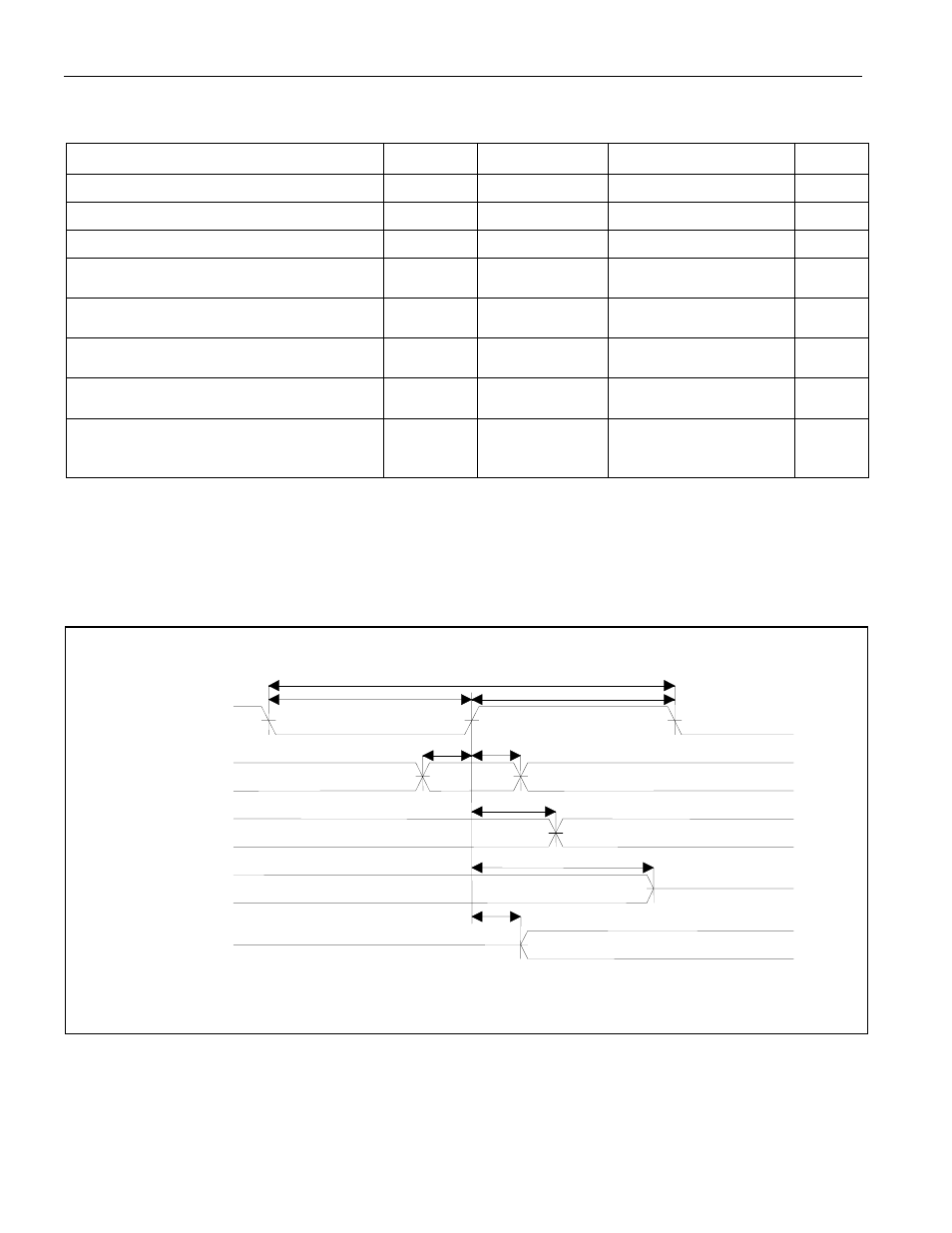
Figure 13-5. PCI Bus Interface AC Timing Diagram
Data Valid
PCLK
PCI Input
and I/O
PCI Output
and I/O
PCI Output and
I/O to Three-state
PCI Output and
I/O from Three-state
Data Valid
Three-state
Three-state
t4
t5
t6
t7
t8
t1
t2
t3