Ac characteristics, Mechanical dimensions, Absolute maximum ratings – Rainbow Electronics DS3131 User Manual
Page 161: Recommended dc operating conditions, Dc characteristics
DS3131
161 of 174
13. AC
CHARACTERISTICS
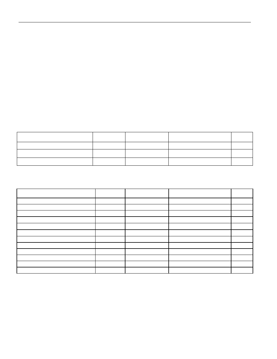
ABSOLUTE MAXIMUM RATINGS
Voltage on Any Lead with Respect to V
SS
(except V
DD
) -0.3V
to
5.5V
Supply Voltage (V
DD
) with Respect to V
SS
-0.3V
to
3.63V
Operating Temperature/Ambient Temperature Under Bias
0°C to +70°C
Junction Temperature Under Bias
≤
125°C
Storage Temperature Range
-55°C to +125°C
Soldering Temperature Range
See IPC/JEDEC J-STD-020A
ESD Tolerance (Note 1)
Class 2 (2000V→4000V HBM:
1.5kΩ,100pF)
Stresses beyond those listed under “Absolute Maximum Ratings” may cause permanent damage to the device. These are stress ratings only,
and functional operation of the device at these or any other conditions beyond those indicated in the operational sections of the specifications is
not implied. Exposure to absolute maximum rating conditions for extended periods may affect device reliability.
RECOMMENDED DC OPERATING CONDITIONS
(T
A
= 0°C to +70°C)
PARAMETER SYMBOL
CONDITIONS
MIN
TYP
MAX
UNITS
Logic 1
V
IH
(Notes 2, 3, 4)
2.2
5.5
V
Logic 0
V
IL
(Note 2)
-0.3
+0.8
V
Supply
V
DD
3.0
3.6
V
DC CHARACTERISTICS
(V
DD
= 3.0V to 3.6V, T
A
= 0°C to +70°C.)
PARAMETER SYMBOL
CONDITIONS
MIN
TYP
MAX
UNITS
Supply Current at V
DD
= 3.6V
I
DD
(Note
5)
200 mA
Pin Capacitance
C
IO
7
pF
Schmitt Hysteresis
V
TH
0.6
V
Input Leakage
I
IL
(Note 6)
-10 +10
µ
A
Input Leakage (with pullups)
I
ILP
(Note 6)
-500 +500
µ
A
Output Leakage
I
LO
(Note 7)
-10 +10
µ
A
Output Current (2.4V)
I
OH
-4.0
mA
Output Current (0.4V)
I
OL
+4.0
mA
Output Current (2.4V), PCI Outputs
I
OH
-8.0
mA
Output Current (0.4V), PCI Outputs
I
OL
+8.0
mA
Output Capacitance
C
OUT
(Note
8)
25 pF
Output Capacitance
C
OUTB
(Note
8)
50 pF
Note 1:
Dallas Semiconductor Communications devices are tested in accordance with ESDA STM 5.1-1998.
Note 2:
Assumes a reasonably noise-free environment.
Note 3:
The PCI 2.1 Specification states that V
IH
should be V
DD
/2 iin a 3.3V signaling environment, and 2.0V in a 5V signaling environment. This
is noncompliance.
Note 4:
The typical values listed above are not production tested.
Note 5:
Measured 170mA with RC0 to RC39 and TC0 to TC39 = 2.048MHz, PCLK = 33MHz, constant traffic on all ports.
Note 6:
0V < V
IN
< V
DD
Note 7:
Outputs in three-state.
Note 8:
C
OUTB
refers to bus-related outputs (PCI and local bus); C
OUT
refers to all other outputs.