D.4 csnadl (ucsadl) – Intel 386 User Manual
Page 574
D-9
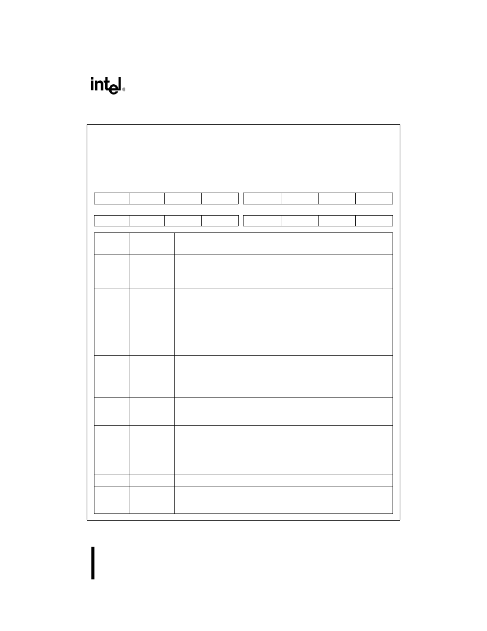
SYSTEM REGISTER QUICK REFERENCE
D.4
CS
nADL (UCSADL)
Chip-select Low Address
CS
nADL (n = 0–6), UCSADL
(read/write)
Expanded Addr:
ISA Addr:
Reset State:
F400H, F408H
F410H, F418H
F420H, F428H
F430H, F438H
—
0000H (CS
nADL)
FF6FH (UCSADL)
15
8
CA5
CA4
CA3
CA2
CA1
CASMM
BS16
MEM
7
0
RDY
—
—
WS4
WS3
WS2
WS1
WS0
Bit
Number
Bit
Mnemonic
Function
15–11
CA5:1
Chip-select Address Value Lower Bits:
Defines the lower 5 bits of the channel’s 15-bit address. The address bits
CA5:1 and the mask bits CM5:1 form a masked address that is compared to
memory address bits A15:11 or I/O address bits A5:1.
10
CASMM
SMM Address Bit:
If this bit is set (and unmasked), the CSU activates the chip-select channel
only while the processor is in SMM (and not in a hold state). Otherwise, the
CSU activates the channel only when processor is operating in a mode
other than SMM.
Setting the SMM mask bit in the channel’s mask low register masks this bit.
When this bit is masked, an address match activates the chip-select,
regardless of whether the processor is in SMM or not.
9
BS16
Bus Size 16-bit:
0 = All bus cycles to addresses in the channel’s address block are byte-
wide.
1 = Bus cycles are 16 bits unless the bus size control pin (BS8#) is
asserted.
8
MEM
Bus Cycle Type:
0 = Configures the channel for an I/O addresses
1 = Configures the channel for memory addresses
7
RDY
Bus Ready Enable:
0 = External READY# is ignored. READY# generated by CSU to terminate
the bus cycle.
1 = Requires that external READY# be active to complete a bus cycle. This
bit must be set to extend wait states beyond the number determined by
WS4:0 (see “Bus Cycle Length Control” on page 14-11).
6–5
—
Reserved; for compatibility with future devices, write zeros to these bits.
4–0
WS4:0
Wait State Value:
WS4:0 defines the minimum number of wait states inserted into the bus
cycle. A zero value means no wait states.