4 register description, 1 mcucr – mcu control register, 2 portb – port b data register – Rainbow Electronics ATmega64M1 User Manual
Page 84: 3 ddrb – port b data direction register, 4 pinb – port b input pins address, 5 portc – port c data register, 6 ddrc – port c data direction register, 7 pinc – port c input pins address, D in “register description, Register
84
8209A–AVR–08/09
ATmega16M1/32M1/64M1
14.4
Register Description
14.4.1
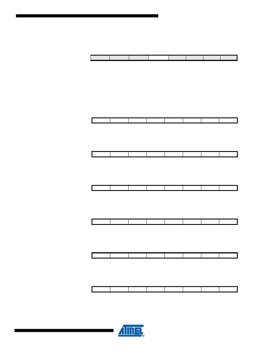
MCUCR – MCU Control Register
• Bit 4 – PUD: Pull-up Disable
When this bit is written to one, the pull-ups in the I/O ports are disabled even if the DDxn and
PORTxn Registers are configured to enable the pull-ups ({DDxn, PORTxn} = 0b01). See
for more details on this feature.
14.4.2
PORTB – Port B Data Register
14.4.3
DDRB – Port B Data Direction Register
14.4.4
PINB – Port B Input Pins Address
14.4.5
PORTC – Port C Data Register
14.4.6
DDRC – Port C Data Direction Register
14.4.7
PINC – Port C Input Pins Address
Bit
7
6
5
4
3
2
1
0
SPIPS
–
–
PUD
–
–
IVSEL
IVCE
MCUCR
Read/Write
R/W
R
R
R/W
R
R
R/W
R/W
Initial Value
0
0
0
0
0
0
0
0
Bit
7
6
5
4
3
2
1
0
PORTB7
PORTB6
PORTB5
PORTB4
PORTB3
PORTB2
PORTB1
PORTB0
PORTB
Read/Write
R/W
R/W
R/W
R/W
R/W
R/W
R/W
R/W
Initial Value
0
0
0
0
0
0
0
0
Bit
7
6
5
4
3
2
1
0
DDB7
DDB6
DDB5
DDB4
DDB3
DDB2
DDB1
DDB0
DDRB
Read/Write
R/W
R/W
R/W
R/W
R/W
R/W
R/W
R/W
Initial Value
0
0
0
0
0
0
0
0
Bit
7
6
5
4
3
2
1
0
PINB7
PINB6
PINB5
PINB4
PINB3
PINB2
PINB1
PINB0
PINB
Read/Write
R/W
R/W
R/W
R/W
R/W
R/W
R/W
R/W
Initial Value
N/A
N/A
N/A
N/A
N/A
N/A
N/A
N/A
Bit
7
6
5
4
3
2
1
0
PORTC7
PORTC6
PORTC5
PORTC4
PORTC3
PORTC2
PORTC1
PORTC0
PORTC
Read/Write
R/W
R/W
R/W
R/W
R/W
R/W
R/W
R/W
Initial Value
0
0
0
0
0
0
0
0
Bit
7
6
5
4
3
2
1
0
DDC7
DDC6
DDC5
DDC4
DDC3
DDC2
DDC1
DDC0
DDRC
Read/Write
R/W
R/W
R/W
R/W
R/W
R/W
R/W
R/W
Initial Value
0
0
0
0
0
0
0
0
Bit
7
6
5
4
3
2
1
0
PINC7
PINC6
PINC5
PINC4
PINC3
PINC2
PINC1
PINC0
PINC
Read/Write
R/W
R/W
R/W
R/W
R/W
R/W
R/W
R/W
Initial Value
N/A
N/A
N/A
N/A
N/A
N/A
N/A
N/A