3 use of adc amplifiers, 4 register description, 1 ac0con – analog comparator 0 control register – Rainbow Electronics ATmega64M1 User Manual
Page 258
258
8209A–AVR–08/09
ATmega16M1/32M1/64M1
24.3
Use of ADC Amplifiers
Thanks to AMPCMP0 configuration bit, Comparator 0 positive input can be connected to Ampli-
fier O output. In that case, the clock of comparator 0 is adapted to the amplifier 0 clock.
“AMP0CSR – Amplifier 0 Control and Status register” on page 249.
Thanks to AMPCMP1 configuration bit, Comparator 1 positive input can be connected to Ampli-
fier 1 output. In that case, the clock of comparator 1 is adapted to the amplifier 1 clock.
“AMP1CSR – Amplifier 1 Control and Status register” on page 250.
Thanks to AMPCMP2 configuration bit, Comparator 2 positive input can be connected to Ampli-
fier 2 output. In that case, the clock of comparator 2 is adapted to the amplifier 2 clock.
“AMP1CSR – Amplifier 1 Control and Status register” on page 250.
24.4
Register Description
Each analog comparator has its own control register. A dedicated register has been designed to
consign the outputs and the flags of the 4 analog comparators.
24.4.1
AC0CON – Analog Comparator 0 Control Register
• Bit 7– AC0EN: Analog Comparator 0 Enable Bit
Set this bit to enable the analog comparator 0.
Clear this bit to disable the analog comparator 0.
• Bit 6– AC0IE: Analog Comparator 0 Interrupt Enable bit
Set this bit to enable the analog comparator 0 interrupt.
Clear this bit to disable the analog comparator 0 interrupt.
• Bit 5:4– AC0IS[1:0]: Analog Comparator 0 Interrupt Select bit
These 2 bits determine the sensitivity of the interrupt trigger.
The different setting are shown in
• Bit 3 – ACCKSEL: Analog Comparator Clock Select
Set this bit to use the PLL output as comparator clock.
Clear this bit to use the CLK
IO
as comparator clock.
• Bit 2: 0– AC0M[2:0]: Analog Comparator 0 Multiplexer register
These 3 bits determine the input of the negative input of the analog comparator.
The different setting are shown in
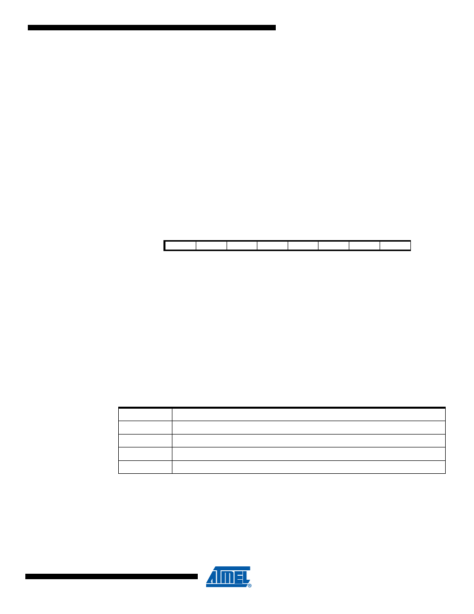
Bit
7
6
5
4
3
2
1
0
AC0EN
AC0IE
AC0IS1
AC0IS0
ACCKSEL
AC0M2
AC0M1
AC0M0
AC0CON
Read/Write
R/W
R/W
R/W
R/W
R/W
R/W
R/W
R/W
Initial Value
0
0
0
0
0
0
0
0
Table 24-1.
Interrupt sensitivity selection
AC0IS[1:0]
Description
00
Comparator Interrupt on output toggle
01
Reserved
10
Comparator interrupt on output falling edge
11
Comparator interrupt on output rising edge