3 data polling eeprom, Sck. see, Figure 28-11 – Rainbow Electronics ATmega64M1 User Manual
Page 307: Table 28-18, Table 28-17
307
8209A–AVR–08/09
ATmega16M1/32M1/64M1
28.10.3
Data Polling EEPROM
When a new byte has been written and is being programmed into EEPROM, reading the
address location being programmed will give the value 0xFF. At the time the device is ready for
a new byte, the programmed value will read correctly. This is used to determine when the next
byte can be written. This will not work for the value 0xFF, but the user should have the following
in mind: As a chip-erased device contains 0xFF in all locations, programming of addresses that
are meant to contain 0xFF, can be skipped. This does not apply if the EEPROM is re-pro-
grammed without chip erasing the device. In this case, data polling cannot be used for the value
0xFF, and the user will have to wait at least t
WD_EEPROM
before programming the next byte. See
for t
WD_EEPROM
value.
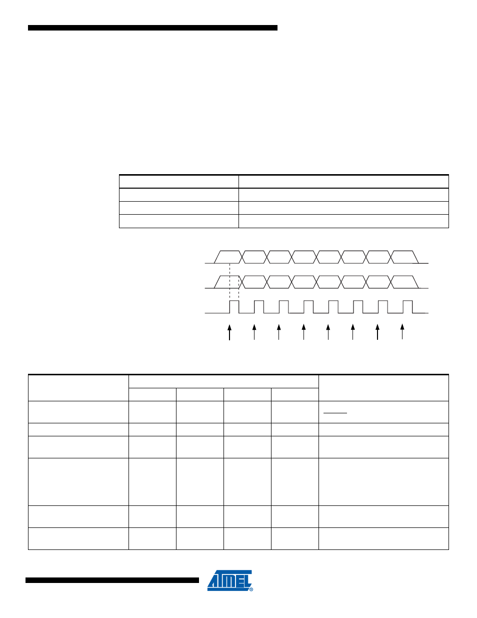
Figure 28-11. Serial Programming Waveforms
Table 28-17. Minimum Wait Delay Before Writing the Next Flash or EEPROM Location
Symbol
Minimum Wait Delay
t
WD_FLASH
4.5 ms
t
WD_EEPROM
3.6 ms
t
WD_ERASE
9.0 ms
MSB
MSB
LSB
LSB
SERIAL CLOCK INPUT
(SCK)
SERIAL DATA INPUT
(MOSI)
(MISO)
SAMPLE
SERIAL DATA OUTPUT
Table 28-18. Serial Programming Instruction Set
Instruction
Instruction Format
Operation
Byte 1
Byte 2
Byte 3
Byte4
Programming Enable
1010 1100
0101 0011
xxxx xxxx
xxxx xxxx
Enable Serial Programming after
RESET goes low.
Chip Erase
1010 1100
100x xxxx
xxxx xxxx
xxxx xxxx
Chip Erase EEPROM and Flash.
Read Program Memory
0010 H000
000a aaaa
bbbb bbbb
oooo oooo
Read H (high or low) data o from
Program memory at word address a:b.
Load Program Memory Page
0100 H000
000x xxxx
xxbb bbbb
iiii iiii
Write H (high or low) data i to Program
Memory page at word address b. Data
low byte must be loaded before Data
high byte is applied within the same
address.
Write Program Memory Page
0100 1100
000a aaaa
bb
xx xxxx
xxxx xxxx
Write Program Memory Page at
address a:b.
Read EEPROM Memory
1010 0000
000x xxaa
bbbb bbbb
oooo oooo
Read data o from EEPROM memory at
address a:b.