7 on-chip debug system, 9 register description, 1 smcr – sleep mode control register – Rainbow Electronics ATmega64M1 User Manual
Page 41: Activated by the sleep instruction. see, Table 10-2
41
8209A–AVR–08/09
ATmega16M1/32M1/64M1
the I/O clock (clk
I/O
) and the ADC clock (clk
ADC
) are stopped, the input buffers of the device will
be disabled. This ensures that no power is consumed by the input logic when not needed. In
some cases, the input logic is needed for detecting wake-up conditions, and it will then be
enabled. Refer to the section
for details on which pins are enabled. If the
input buffer is enabled and the input signal is left floating or have an analog signal level close to
V
CC
/2, the input buffer will use excessive power.
For analog input pins, the digital input buffer should be disabled at all times. An analog signal
level close to V
CC
/2 on an input pin can cause significant current even in active mode. Digital
input buffers can be disabled by writing to the Digital Input Disable Registers (DIDR1 and
DIDR0). Refer to “DIDR1 – Digital Input Disable Register 1” and “DIDR0 – Digital Input Disable
Register 0” on
for details.
10.8.7
On-chip Debug System
If the On-chip debug system is enabled by OCDEN Fuse and the chip enter sleep mode, the
main clock source is enabled, and hence, always consumes power. In the deeper sleep modes,
this will contribute significantly to the total current consumption.
10.9
Register Description
10.9.1
SMCR – Sleep Mode Control Register
The Sleep Mode Control Register contains control bits for power management.
• Bits 7:4 -
Res: Reserved
These bits are reserved and will always read as zero.
• Bits 3:1 – SM[2:0]: Sleep Mode Select Bits 2, 1, and 0
These bits select between the five available sleep modes as shown in
.
Note:
1. Standby mode is only recommended for use with external crystals or resonators.
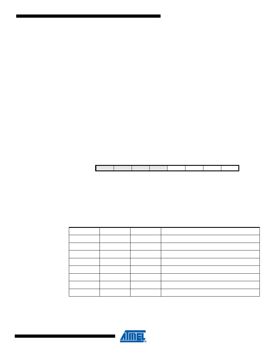
Bit
7
6
5
4
3
2
1
0
–
–
–
–
SM2
SM1
SM0
SE
SMCR
Read/Write
R
R
R
R
R/W
R/W
R/W
R/W
Initial Value
0
0
0
0
0
0
0
0
Table 10-2.
Sleep Mode Select
SM2
SM1
SM0
Sleep Mode
0
0
0
Idle
0
0
1
ADC Noise Reduction
0
1
0
Power-down
0
1
1
Reserved
1
0
0
Reserved
1
0
1
Reserved
1
1
0
Standby
1
1
1
Reserved