3 tccr1c – timer/counter1 control register c – Rainbow Electronics ATmega64M1 User Manual
Page 127
127
8209A–AVR–08/09
ATmega16M1/32M1/64M1
When the ICRn is used as TOP value (see description of the WGMn3:0 bits located in the
TCCRnA and the TCCRnB Register), the ICPn is disconnected and consequently the Input Cap-
ture function is disabled.
• Bit 5 –
RTGEN
Set this bit to enable the ICP1A as a timer/counter retrigger input.
(This bit is reserved for future use. For ensuring compatibility with future devices, this bit must be
written to zero when TCCRnB is written.)
• Bit 4:3 – WGMn3:2: Waveform Generation Mode
See TCCRnA Register description.
• Bit 2:0 – CSn2:0: Clock Select
The three Clock Select bits select the clock source to be used by the Timer/Counter, see
and
.
If external pin modes are used for the Timer/Countern, transitions on the Tn pin will clock the
counter even if the pin is configured as an output. This feature allows software control of the
counting.
16.11.3
TCCR1C – Timer/Counter1 Control Register C
• Bit 7 – FOCnA: Force Output Compare for Channel A
• Bit 6 – FOCnB: Force Output Compare for Channel B
The FOCnA/FOCnB bits are only active when the WGMn3:0 bits specifies a non-PWM mode.
However, for ensuring compatibility with future devices, these bits must be set to zero when
TCCRnA is written when operating in a PWM mode. When writing a logical one to the
FOCnA/FOCnB bit, an immediate compare match is forced on the Waveform Generation unit.
The OCnA/OCnB output is changed according to its COMnx1:0 bits setting. Note that the
FOCnA/FOCnB bits are implemented as strobes. Therefore it is the value present in the
COMnx1:0 bits that determine the effect of the forced compare.
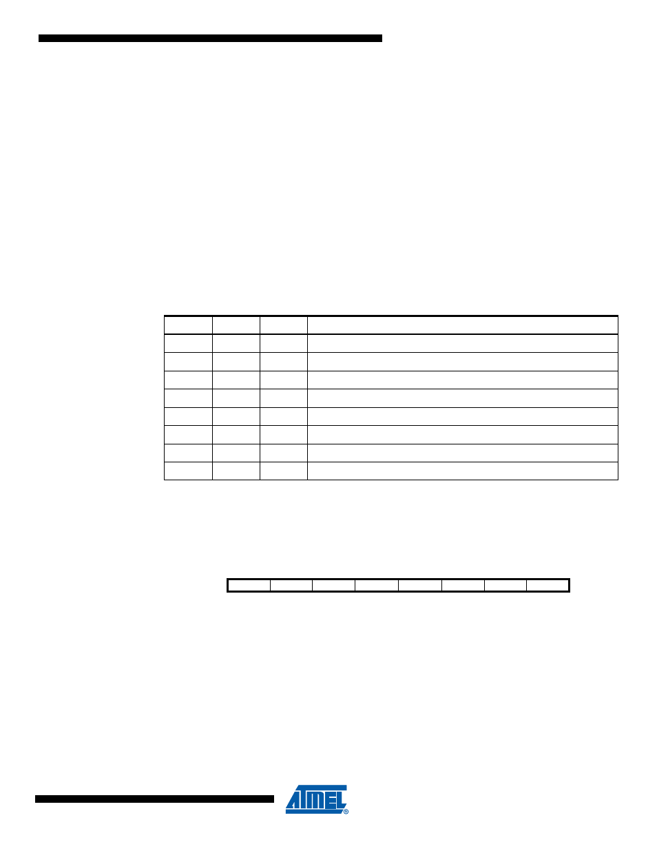
Table 16-5.
Clock Select Bit Description
CSn2
CSn1
CSn0
Description
0
0
0
No clock source (Timer/Counter stopped).
0
0
1
clk
I/O
/1 (No prescaling)
0
1
0
clk
I/O
/8 (From prescaler)
0
1
1
clk
I/O
/64 (From prescaler)
1
0
0
clk
I/O
/256 (From prescaler)
1
0
1
clk
I/O
/1024 (From prescaler)
1
1
0
External clock source on Tn pin. Clock on falling edge.
1
1
1
External clock source on Tn pin. Clock on rising edge.
Bit
7
6
5
4
3
2
1
0
FOC1A
FOC1B
–
–
–
–
–
–
TCCR1C
Read/Write
R/W
R/W
R
R
R
R
R
R
Initial Value
0
0
0
0
0
0
0
0