3 tcnt0 – timer/counter register, 4 ocr0a – output compare register a, 5 ocr0b – output compare register b – Rainbow Electronics ATmega64M1 User Manual
Page 101: 6 timsk0 – timer/counter interrupt mask register
101
8209A–AVR–08/09
ATmega16M1/32M1/64M1
If external pin modes are used for the Timer/Counter0, transitions on the T0 pin will clock the
counter even if the pin is configured as an output. This feature allows software control of the
counting.
15.9.3
TCNT0 – Timer/Counter Register
The Timer/Counter Register gives direct access, both for read and write operations, to the
Timer/Counter unit 8-bit counter. Writing to the TCNT0 Register blocks (removes) the Compare
Match on the following timer clock. Modifying the counter (TCNT0) while the counter is running,
introduces a risk of missing a Compare Match between TCNT0 and the OCR0x Registers.
15.9.4
OCR0A – Output Compare Register A
The Output Compare Register A contains an 8-bit value that is continuously compared with the
counter value (TCNT0). A match can be used to generate an Output Compare interrupt, or to
generate a waveform output on the OC0A pin.
15.9.5
OCR0B – Output Compare Register B
The Output Compare Register B contains an 8-bit value that is continuously compared with the
counter value (TCNT0). A match can be used to generate an Output Compare interrupt, or to
generate a waveform output on the OC0B pin.
15.9.6
TIMSK0 – Timer/Counter Interrupt Mask Register
• Bits 7:3 – Res: Reserved
These bits are reserved and will always read as zero.
1
0
0
clk
I/O
/256 (From prescaler)
1
0
1
clk
I/O
/1024 (From prescaler)
1
1
0
External clock source on T0 pin. Clock on falling edge.
1
1
1
External clock source on T0 pin. Clock on rising edge.
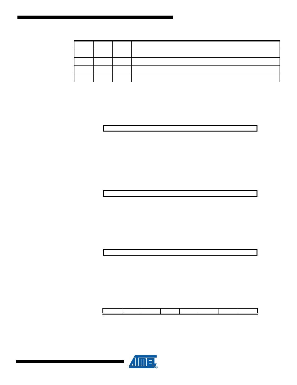
Table 15-9.
Clock Select Bit Description (Continued)
CS02
CS01
CS00
Description
Bit
7
6
5
4
3
2
1
0
TCNT0[7:0]
TCNT0
Read/Write
R/W
R/W
R/W
R/W
R/W
R/W
R/W
R/W
Initial Value
0
0
0
0
0
0
0
0
Bit
7
6
5
4
3
2
1
0
OCR0A[7:0]
OCR0A
Read/Write
R/W
R/W
R/W
R/W
R/W
R/W
R/W
R/W
Initial Value
0
0
0
0
0
0
0
0
Bit
7
6
5
4
3
2
1
0
OCR0B[7:0]
OCR0B
Read/Write
R/W
R/W
R/W
R/W
R/W
R/W
R/W
R/W
Initial Value
0
0
0
0
0
0
0
0
Bit
7
6
5
4
3
2
1
0
–
–
–
–
–
OCIE0B
OCIE0A
TOIE0
TIMSK0
Read/Write
R
R
R
R
R
R/W
R/W
R/W
Initial Value
0
0
0
0
0
0
0
0