2 analog noise canceling techniques, In figure 22-8 – Rainbow Electronics ATmega64M1 User Manual
Page 233
233
8209A–AVR–08/09
ATmega16M1/32M1/64M1
to remove high frequency components with a low-pass filter before applying the signals as
inputs to the ADC.
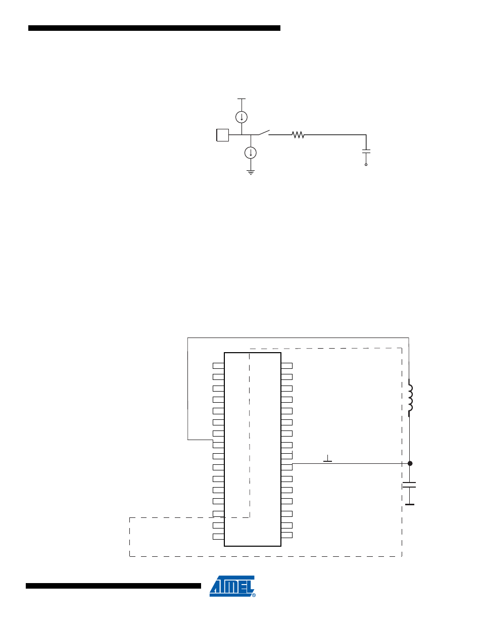
Figure 22-8. Analog Input Circuitry
22.6.2
Analog Noise Canceling Techniques
Digital circuitry inside and outside the device generates EMI which might affect the accuracy of
analog measurements. If conversion accuracy is critical, the noise level can be reduced by
applying the following techniques:
1.
Keep analog signal paths as short as possible. Make sure analog tracks run over the
analog ground plane, and keep them well away from high-speed switching digital
tracks.
2.
The AV
CC
pin on the device should be connected to the digital V
CC
supply voltage via an
LC network as shown in
.
3.
Use the ADC noise canceler function to reduce induced noise from the CPU.
4.
If any ADC port pins are used as digital outputs, it is essential that these do not switch
while a conversion is in progress.
Figure 22-9. ADC Power Connections
ADCn
I
IH
1..100 k
Ω
C
S/H
= 14 pF
V
CC
/2
I
IL
1
2
3
4
5
6
7
8
9
10
11
12
13
14
15
16
32
31
30
29
28
27
26
25
24
23
22
21
20
19
18
17
VCC
GND
(ACMPN3/ADC0) PE2
(ADC1) PD4
PB7(ADC4)
PB6 (ADC7)
PB5 (ADC6/ACMPN1/AMP2-)
PC7 (D2A/AMP2+)
PB4 (AMP0+)
PB3 (AMP0-)
PC6 (ADC10/ACMP1)
AREF (ISRC)
AGND
AVCC
PC5 (ADC9/ACMP3/AMP1+)
PC4 (ADC8/AMP1-)
PB2 (ADC5/ACMPN0)
PD7 (ACMP0)
PD6 (ADC3/ACMPN2)
PD5 (ADC2/ACMP2)
100nF
Analog Ground Plane
10
μH