Rainbow Electronics ATmega64M1 User Manual
Page 249

249
8209A–AVR–08/09
ATmega16M1/32M1/64M1
• Bit 6:0 – ADC10D..8D, ACMP0D, ACMP1D, ACMP3D, AMP0PD, AMP0ND, AMP1PD,
AMP1ND, AMP2PD:
ADC10..8, ACMP0, ACMP1, ACMP3, AMP0P, AMP0N, AMP1P, AMP1N, AMP2P Digital
Input Disable
When this bit is written logic one, the digital input buffer on the corresponding ADC pin is dis-
abled. The corresponding PIN Register bit will always read as zero when this bit is set. When an
analog signal is applied to an analog pin and the digital input from this pin is not needed, this bit
should be written logic one to reduce power consumption in the digital input buffer.
22.10.8
AMP0CSR – Amplifier 0 Control and Status register
• Bit 7 – AMP0EN: Amplifier 0 Enable Bit
Set this bit to enable the Amplifier 0.
Clear this bit to disable the Amplifier 0.
Clearing this bit while a conversion is running will take effect at the end of the conversion.
Warning: Always clear AMP0TS0:1 when clearing AMP0EN.
• Bit 6 – AMP0IS: Amplifier 0 Input Shunt
Set this bit to short-circuit the Amplifier 0 input.
Clear this bit to normally use the Amplifier 0.
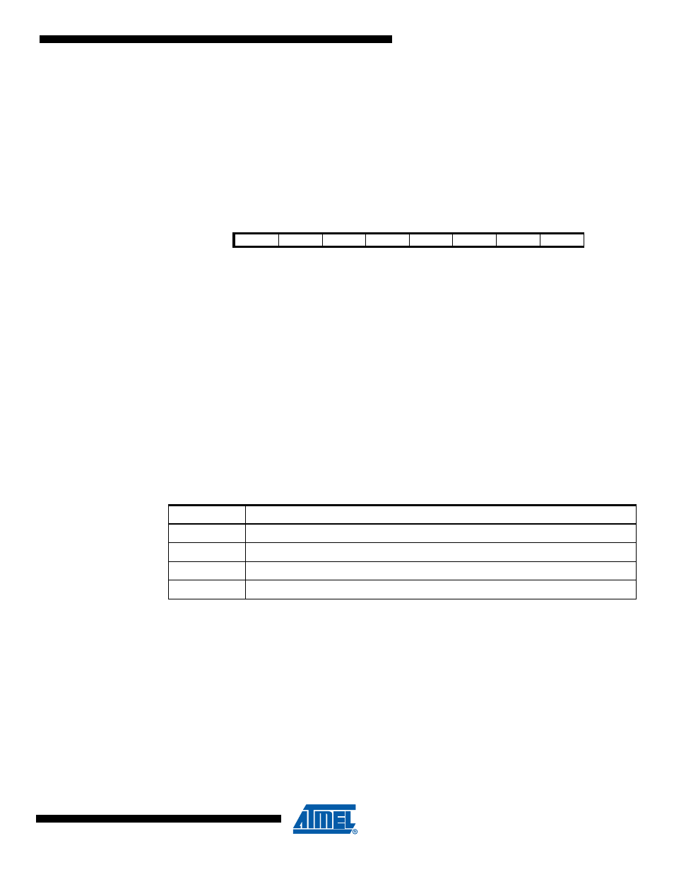
• Bit 5:4 – AMP0G[1:0]: Amplifier 0 Gain Selection Bits
These 2 bits determine the gain of the amplifier 0.
The different setting are shown in
To ensure an accurate result, after the gain value has been changed, the amplifier input needs
to have a quite stable input value during at least 4 Amplifier synchronization clock periods.
• Bit 3 – AMPCMP0: Amplifier 0 - Comparator 0 connection
Set this bit to connect the amplifier 0 to the comparator 0 positive input. In this configuration the
comparator clock is adapted to the amplifier clock and AMP0TS[2:0] bits have no effect.
Clear this bit to normally use the Amplifier 0.
• Bit 2:0 – AMP0TS[2:0]: Amplifier 0 Clock Source Selection Bits
In accordance with the
, these 3 bits select the event which will generate the clock for
the amplifier 0. This clock source is necessary to start the conversion on the amplified channel.
Bit
7
6
5
4
3
2
1
0
AMP0EN
AMP0IS
AMP0G1
AMP0G0
AMPCMP0
AMP0TS2
AMP0TS1
AMP0TS0
AMP0CSR
Read/Write
R/W
R/W
R/W
R/W
R/W
R/W
R/W
R/W
Initial Value
0
0
0
0
0
0
0
0
Table 22-8.
Amplifier 0 Gain Selection
AMP0G[1:0]
Description
00
Gain 5
01
Gain 10
10
Gain 20
11
Gain 40
