Comtech EF Data DMD20 User Manual
Page 39
DMD20/DMD50/DMD2050/DMD2050E/DMD1050/OM20 Remote Protocol
Remote Operations
MN-DMDREMOTEOP Revision 9
1–29
<1>
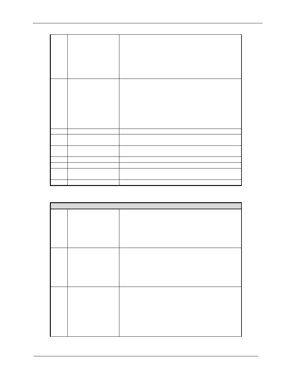
Alarm 4
Bit 0 = LBST BUC DC Current Alarm, 1 = Fail
Bit 1 = LBST BUC DC Voltage Alarm, 1 = Fail
Bit 2 = Ethernet WAN Alarm, 1 = Fail
Bit 3 = LBST BUC PLL Alarm, 1 = Fail
Bit 4 = LBST BUC Over Temperature Alarm, 1 = Fail
Bit 5 = LBST BUC Summary Alarm, 1 = Fail
Bit 6 = LBST BUC Output Enable Alarm, 1 = Fail
Bit 7 = LBST BUC Communications Alarm, 1 = Fail
<1>
Latched Alarm 4
Bit 0 = LBST BUC DC Current Alarm
Bit 1 = LBST BUC DC Voltage Alarm
Bit 2 = Ethernet WAN Alarm
Bit 3 = LBST BUC PLL Alarm
Bit 4 = LBST BUC Over Temperature Alarm
Bit 5 = LBST BUC Summary Alarm
Bit 6 = LBST BUC Output Enable Alarm
Bit 7 = LBST BUC Communications Alarm
0 = Not Latched, 1 = Latched
<1> Reserved
Ignore
<2>
LBST BUC DC
Current
Amps, Implied decimal point, 1000 = 1.000A
<2>
LBST BUC DC
Voltage
Volts, Implied decimal point, 10 = 1.0V
<1>
FSK Test Result
0 = Pass, 1 = Fail
<2>
BUC Carrier Level
Implied decimal point, dBm
<4> BUC
Summary
Status
<1>
BUC Temperature
Implied Decimal Point, C
Opcode: <2405h>
Query a Modulator's Latched Alarms
Query Response (5 Bytes)
<1>
Latched Alarm 1
Bit 0 = Transmit FPGA/Processor Fault
Bit 1 = Drop DSP
Bit 2 = Transmit Symbol Clock PLL Lock
Bit 3 = Reserved
Bit 4 = Transmit L-Band Synthesizer Lock
Bits 5 – 7 = Reserved
0 = Not Latched, 1 = Latched
<1> Latched
Common
Alarm 1
Bit 0 = -12V Alarm
Bit 1 = +12V Alarm
Bit 2 = +5V Alarm
Bits 3 – 5 = Reserved
Bit 6 = IF SYNTH Alarm
Bit 7 = Spare
0 = Not Latched, 1 = Latched
<1> Latched
Common
Alarm 2
Bit 0 = TERR FPGA Config
Bit 1 = CODEC FPGA Config
Bit 2 = CODEC Device Config
Bit 3 = TRANSEC Power Test
Bit 4 = +1.5 V Rx Alarm
Bit 5 = +1.5 V TX Alarm
Bit 6 = +3.3 V Alarm
Bit 7 = +20 V Alarm
0 = Not Latched, 1 = Latched