2 lcd contrast adjust register (lcra, m2[0ah]), 2 lcd contrast adjust register (lcra, m2[0ah]) -3, Maxq family user’s guide: maxq2010 supplement – Maxim Integrated MAXQ Family Users Guide: MAXQ2010 Supplement User Manual
Page 95
MAXQ Family User’s Guide:
MAXQ2010 Supplement
20-3
Bit 1: Operation Mode (OPM). This bit determines whether the LCD controller is operating (driving SEG and COM
lines) or suspended (with its clock gated off).
0 = The LCD controller is suspended.
1 = The LCD controller is in normal operating mode.
Bit 0: Display Enable (DPE). When the LCD controller is in normal operating mode, this bit controls whether the display
register data is used to drive the LCD. This bit has no meaning when LCD operation is suspended (OPM = 0).
0 = Disables the LCD display. SEG and COM waveforms are driven to turn all segments off.
1 = Drives the LCD display normally.
20.2.2 LCD Contrast Adjust Register (LCRA, M2[0Ah])
This register can only be written to when the LCD controller is in suspended mode (OPM = 0).
Bits 15:13, 4: Reserved
Bits 12:11: LCD Duty-Cycle Select (DUTY[1:0]). These bits select the LCD display duty cycle and corresponding
bias generation mode as follows:
Bits 10:7: LCD Frame Frequency (FRM[3:0]). These bits select the LCD frame frequency as follows:
For 1/3 bias mode:
f
FRAME
= f
LCD
/((FRM[3:0]) + 1) x 96)
For all other modes:
f
FRAME
= f
LCD
/((FRM[3:0]) + 1) x 64)
Bit 6: LCD Clock Select (LCCS). This bit selects the source clock (f
LCD
) used for LCD segment and common timing
generation.
0 = f
LCD
= 32kHz clock
1 = f
LCD
= high-frequency oscillator/512
Note: Because the high-frequency clock is halted when stop mode is invoked, LCD operation from the divided
high-frequency clock (LCCS = 1) during stop mode is not possible. The user is advised to suspend LCD opera-
tion before entering stop mode or use the 32kHz for frame frequency generation if LCD operation is required
during stop mode.
Bit 5: LCD Resistor Internally Grounded (LRIG)
0 = R
ADJ
is disconnected from ground internally.
1 = R
ADJ
is connected to ground internally.
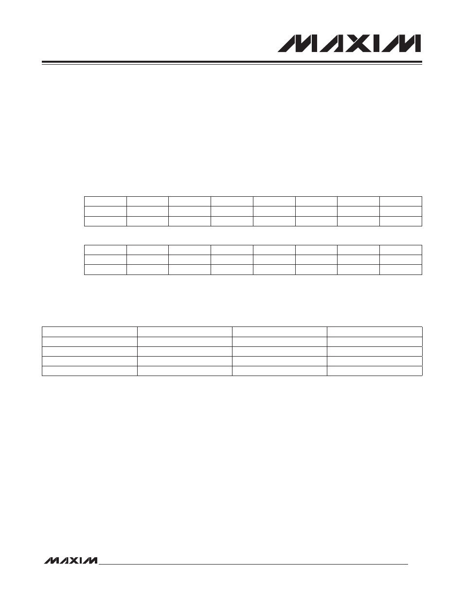
Bit #
15
14
13
12
11
10
9
8
Name
—
—
—
DUTY1
DUTY0
FRM3
FRM2
FRM1
Reset
0
0
0
0
0
0
0
0
Access
r
r
r
rw
rw
rw
rw
rw
Bit #
7
6
5
4
3
2
1
0
Name
FRM0
LCCS
LRIG
—
LRA3
LRA2
LRA1
LRA0
Reset
0
0
0
0
0
0
0
0
Access
rw
rw
rw
rw
rw
rw
rw
rw
DUTY1
DUTY0
DUTY CYCLE
BIAS MODE
0
0
Static
Static
0
1
1/2
1/2
1
0
1/3
1/3
1
1
1/4
1/3