7 lcd internal adjustable contrast resistor, 7 lcd internal adjustable contrast resistor -8, Figure 20-2. lcd drive voltage generation -8 – Maxim Integrated MAXQ Family Users Guide: MAXQ2010 Supplement User Manual
Page 100: Table 20-1. lcd display modes -8, Maxq family user’s guide: maxq2010 supplement, Table 20-1. lcd display modes
MAXQ Family User’s Guide:
MAXQ2010 Supplement
20-8
20.7 LCD Internal Adjustable Contrast Resistor
For an LCD segment to be in the off state, the V
RMS
voltage between its COM and SEG signals must remain below the
threshold voltage for that particular LCD display. As the V
RMS
voltage difference increases, the LCD segment remains
off until the threshold voltage is reached, at which point it turns on. As the V
RMS
difference continues to increase, the
contrast of the LCD segment increases as well (the segment becomes darker).
In order to adjust the visible contrast level for all LCD segments, the internal adjustable resistor R
ADJ
can be varied
between approximately 0 and 80kI by setting the bits LRA[3:0] (LCRA[3:0]). Changing this value causes the difference
between V
LCD
, V
LCD1
, V
LCD2
, and V
ADJ
to increase or decrease evenly for all four drive voltages.
For the internal resistor R
ADJ
to be used in this manner, the LRIG bit must be set to 1 to connect R
ADJ
to ground inter-
nally. If an external adjustable resistor is used for the contrast adjustment function, LRIG should be set to 0 and the
external resistor R
EXT
should be connected between V
ADJ
and ground as shown in Figure 20-3.
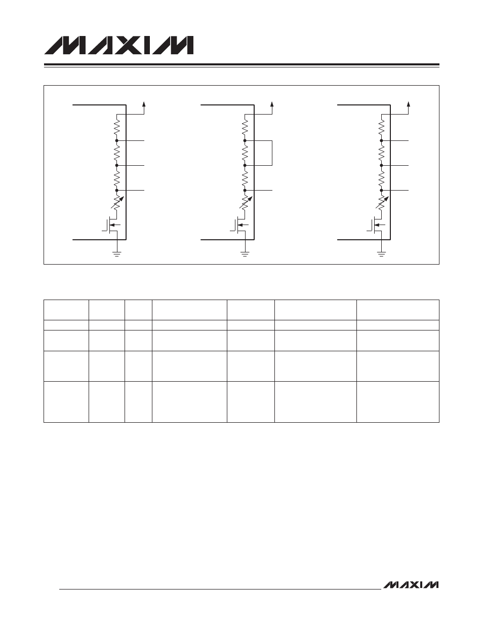
Figure 20-2. LCD Drive Voltage Generation
Table 20-1. LCD Display Modes
*For 1/2 bias mode, this assumes an external shunt in place between V
LCD1
and V
LCD2
.
STATIC DISPLAY
R
R
V
LCD2
V
ADJ
R
V
LCD
V
LCD1
R
ADJ
DGND
LRIG
1/2 BIAS
R
R
V
LCD2
V
ADJ
R
V
LCD
V
LCD1
R
ADJ
DGND
LRIG
1/3 BIAS
R
R
V
LCD2
V
ADJ
R
V
LCD
V
LCD1
R
ADJ
DGND
LRIG
DUTY[1:0]
DUTY
CYCLE
BIAS
DISPLAY SEGMENT
DRIVE CAPACITY
COMMONS
V
LCD2
VOLTAGE*
V
LCD1
VOLTAGE*
00
Static
—
43
COM0
—
—
01
1/2
1/2
84
COM0
COM1
V
ADJ
+ (1/2 x V
LCD
-
V
ADJ
)
V
ADJ
+ (1/2 x V
LCD
-
V
ADJ
)
10
1/3
1/3
123
COM0
COM1
COM2
V
ADJ
+ (1/3 x V
LCD
-
V
ADJ
)
V
ADJ
+ (2/3 x V
LCD
-
V
ADJ
)
11
1/4
1/3
160
COM0
COM1
COM2
COM3
V
ADJ
+ (1/3 x V
LCD
-
V
ADJ
)
V
ADJ
+ (2/3 x V
LCD
-
V
ADJ
)