Maxq family user’s guide: maxq2010 supplement – Maxim Integrated MAXQ Family Users Guide: MAXQ2010 Supplement User Manual
Page 106
MAXQ Family User’s Guide:
MAXQ2010 Supplement
20-14
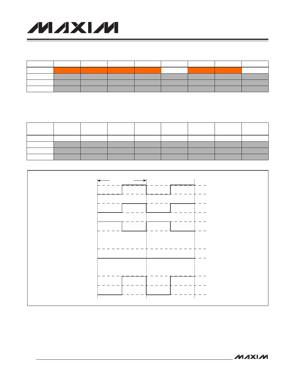
According to the static memory map table, a value of 0F6h should be written to the LCD0 register as shown in Table 20-8.
Table 20-7. Static Drive Example Common Signal Selection
Table 20-8. Static Drive Example Register Content
Figure 20-6. Static Drive Example Waveform Timing
V
LCD
GND
COM0
1 FRAME (f
FRAME
)
V
LCD
GND
SEG0
V
LCD
GND
SEG1
V
LCD
GND
- V
LCD
COM0–SEG1
(ON)
V
LCD
GND
COM0–SEG0
(OFF)
SEG7
SEG6
SEG5
SEG4
SEG3
SEG2
SEG1
SEG0
COM0
On
On
On
On
Off
On
On
Off
COM1
COM2
COM3
BIT 7
COM0
BIT 6
COM0
BIT 5
COM0
BIT 4
COM0
BIT 3
COM0
BIT 2
COM0
BIT 1
COM0
BIT 0
COM0
LCD0
1
1
1
1
0
1
1
0
LCD1
LCD2
LCD3
See also other documents in the category Maxim Integrated Hardware:
- DS80C390 (58 pages)
- DS5001FP (26 pages)
- MAX1416 (14 pages)
- MAX5865 (18 pages)
- DS33Z41 (167 pages)
- MAX1202 (7 pages)
- USBTO232 (31 pages)
- HFAN-09.5.0: Pattern Creator/Converter Software (8 pages)
- MAX-IDE MAXQ Microcontrollers (11 pages)
- MAX6876 Power-Supply Tracker/Sequencer (6 pages)
- MAX6877 Power-Supply Tracker/Sequencer (3 pages)
- 78Q8430 ARM9(920T) Linux Driver Diagnostic Guide (19 pages)
- 78Q8430 Software Driver (54 pages)
- 78Q8430 ST 5100/OS-20 with NexGen TCP/IP Stack (28 pages)
- 6612_OMU_S2_URT_V1_13 (56 pages)
- 6612_OMU_S2+2_URT_V1_14 (58 pages)
- 71M6511 Power Meter IC Family Software (137 pages)
- 71M65xx ADM51 ICE Safety Notice (2 pages)
- 71M6511 2-Layer Demo Board (2 pages)
- 71M6511 4-Layer Demo Board (2 pages)
- 78Q8430 Linux Driver ARM Platform (22 pages)
- 71M6513 Demo Board (2 pages)
- 71M6521DE Energy Meter IC Family Software (138 pages)
- 71M6521 Demo Board (2 pages)
- 71M6531 Demo Board (2 pages)
- 71M6531 Energy Meter IC Family Software (116 pages)
- 71M6533 Demo Board (2 pages)
- 71M6534H Demo Board (2 pages)
- 71M6515H Demo Board (2 pages)
- 73S1209F Evaluation Board (2 pages)
- 73S12xxF (38 pages)
- 73S12xxF Software (93 pages)
- 73S1210F Evaluation Board Lite (2 pages)
- 73S1210F Evaluation Board (2 pages)
- 73S1210F Multi-SAM Evaluation Board Lite (2 pages)
- 73S12xxF USB-CCID Linux DFU Host Application (8 pages)
- 73S1215F Device Firmware Upgrade Host Driver/Application (10 pages)
- 73S12xxF USB-CCID Host GUI (22 pages)
- 73S1215F Windows XP 32 USB CCID and DFU Drivers (15 pages)
- 73S1215F CCID USB Linux Driver (16 pages)
- 73S1215F Evaluation Board (2 pages)
- 73S1215F Evaluation Board Lite (2 pages)
- 73S1217F Evaluation Board (2 pages)
- 73S1217F Evaluation Board Lite (2 pages)
- MAXQ Family (216 pages)