1 timer/counter b register descriptions, 1 timer/counter b register descriptions -2, Maxq family user’s guide: maxq2010 supplement – Maxim Integrated MAXQ Family Users Guide: MAXQ2010 Supplement User Manual
Page 113
MAXQ Family User’s Guide:
MAXQ2010 Supplement
21-2
21.1 Timer/Counter B Register Descriptions
The following peripheral registers are used to control the LCD display controller. Addresses for all registers are given
as “Mx[yy],” where x is the module number (from 0 to 15 decimal) and yy is the register index (from 00h to 1Fh hexa-
decimal). Fields in the bit definition tables are defined as follows:
• Name: Symbolic names of bits or bit fields in this register.
• Reset: The value of each bit in this register following a standard reset. If this field reads “unchanged,” the given bit
is unaffected by standard reset. If this field reads “s,” the given bit does not have a fixed 0 or 1 reset value because
its value is determined by another internal state or external condition.
• POR: If present this field defines the value of each bit in this register following a power-on reset (as opposed to a
standard reset). Some bits are unaffected by standard resets and are set/cleared by POR only.
• Access: Bits can be read-only (r) or read/write (rw). Any special restrictions or conditions that could apply when
reading or writing this bit are detailed in the bit description.
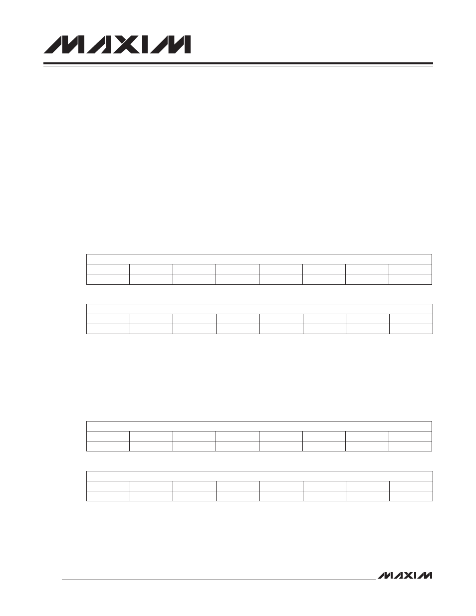
21.1.1 Timer B Timer/Counter 0/1/2 Capture/Reload Register (TB0R, TB1R, TB2R; M4[00h],
M4[02h], M4[04h])
Bits 15:0: Timer B Capture/Reload Register. This register is used to capture the TBnV value when Timer B is config-
ured in capture mode. This register is also used as the 16-bit reload value when Timer B is configured in autoreload
mode.
21.1.2 Timer B Timer/Counter 0/1/2 Compare Register (TB0C, TB1C, TB2C; M4[01h],
M4[03h], M4[05h])
Bits 15:0: Timer B Compare Register. This register is used for comparison vs. the TBnV value when Timer B is oper-
ated in compare mode.
Bit #
15
14
13
12
11
10
9
8
Name
TBnR
Reset
0
0
0
0
0
0
0
0
Access
rw
rw
rw
rw
rw
rw
rw
rw
Bit #
7
6
5
4
3
2
1
0
Name
TBnR
Reset
0
0
0
0
0
0
0
0
Access
rw
rw
rw
rw
rw
rw
rw
rw
Bit #
15
14
13
12
11
10
9
8
Name
TBnC
Reset
0
0
0
0
0
0
0
0
Access
rw
rw
rw
rw
rw
rw
rw
rw
Bit #
7
6
5
4
3
2
1
0
Name
TBnC
Reset
0
0
0
0
0
0
0
0
Access
rw
rw
rw
rw
rw
rw
rw
rw