2 analog-to-digital pins and control registers, 2 analog-to-digital pins and control registers -2, Maxq family user’s guide: maxq2010 supplement – Maxim Integrated MAXQ Family Users Guide: MAXQ2010 Supplement User Manual
Page 84
MAXQ Family User’s Guide:
MAXQ2010 Supplement
19-2
19.2 Analog-to-Digital Pins and Control Registers
Tables 19-1 and 19-2 list the pins and control registers dedicated to the ADC. Note that all ADC pins are dedicated,
so none of them is multiplexed with GPIO port pins. Addresses for all registers are given as “Mx[yy],” where x is the
module number (from 0 to 15 decimal) and yy is the register index (from 00h to 1Fh hexadecimal). Fields in the bit
definition tables are defined as follows:
• Name: Symbolic names of bits or bit fields in this register.
• Reset: The value of each bit in this register following a standard reset. If this field reads “unchanged,” the given bit
is unaffected by standard reset. If this field reads “s,” the given bit does not have a fixed 0 or 1 reset value because
its value is determined by another internal state or external condition.
• POR: If present this field defines the value of each bit in this register following a power-on reset (as opposed to a
standard reset). Some bits are unaffected by standard resets and are set/cleared by POR only.
• Access: Bits can be read-only (r) or read/write (rw). Any special restrictions or conditions that could apply when
reading or writing this bit are detailed in the bit description.
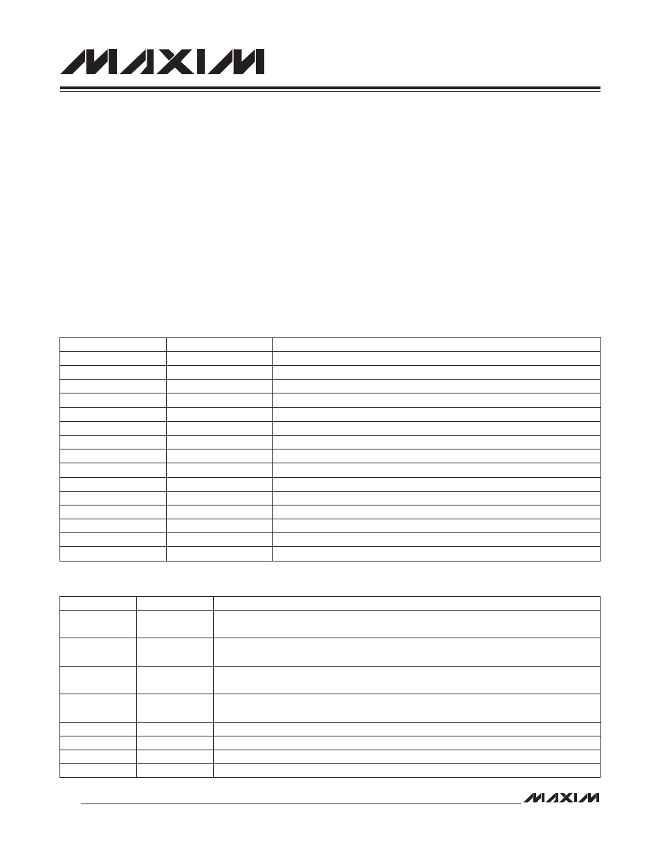
Table 19-1. ADC Input and Power-Supply Pins
Table 19-2. ADC Control Registers
PIN
NAME
ADC INTERFACE FUNCTION
82
AVDD
Analog Supply Voltage
79
AGND
Analog Ground
70
AVREF
External ADC Voltage Reference
78
AN0
Single-Ended Analog Input Channel 0
77
AN1
Single-Ended Analog Input Channel 1
76
AN2
Single-Ended Analog Input Channel 2
75
AN3
Single-Ended Analog Input Channel 3
74
AN4
Single-Ended Analog Input Channel 4
73
AN5
Single-Ended Analog Input Channel 5
72
AN6
Single-Ended Analog Input Channel 6
71
AN7
Single-Ended Analog Input Channel 7
78, 77
(AN0, AN1)
Differential Input Channel 0
76, 75
(AN2, AN3)
Differential Input Channel 1
74, 73
(AN4, AN5)
Differential Input Channel 2
72, 71
(AN6, AN7)
Differential Input Channel 3
REGISTER
ADDRESS
FUNCTION
ADST
M4[06h]
ADC Status Register. Contains the ADCFG and ADBUF register index selection bits,
conversion start bit, and other status bits for the ADC.
ADADDR
M4[07h]
ADC Address Register. Defines the first and last ADCFG registers used in a conversion
sequence as well as the first ADBUF register written in a conversion sequence.
ADCN
M4[0Eh]
ADC Control Register. Controls sample acquisition extend, power-management mode,
single/continuous sequence conversion, interrupt modes, and clock division for the ADC.
ADDATA
M4[0Fh]
ADC Data Register. Acts as a read/write access point to registers ADCFG[0] to ADCFG[7]
and ADBUF[0] to ADBUF[15].
ADCFG[0]
ADDATA[10h]
ADC Sequence Configuration Register 0
ADCFG[1]
ADDATA[11h]
ADC Sequence Configuration Register 1
ADCFG[2]
ADDATA[12h]
ADC Sequence Configuration Register 2
ADCFG[3]
ADDATA[13h]
ADC Sequence Configuration Register 3