2 lcd controller register descriptions, 1 lcd configuration register (lcfg, m2[06h]), 2 lcd controller register descriptions -2 – Maxim Integrated MAXQ Family Users Guide: MAXQ2010 Supplement User Manual
Page 94: 1 lcd configuration register (lcfg, m2[06h]) -2, Maxq family user’s guide: maxq2010 supplement
MAXQ Family User’s Guide:
MAXQ2010 Supplement
20-2
20.2 LCD Controller Register Descriptions
The following peripheral registers are used to control the LCD display controller. Addresses for all registers are given
as “Mx[yy],” where x is the module number (from 0 to 15 decimal) and yy is the register index (from 00h to 1Fh hexa-
decimal). Fields in the bit definition tables are defined as follows:
• Name: Symbolic names of bits or bit fields in this register.
• Reset: The value of each bit in this register following a standard reset. If this field reads “unchanged,” the given bit
is unaffected by standard reset. If this field reads “s,” the given bit does not have a fixed 0 or 1 reset value because
its value is determined by another internal state or external condition.
• POR: If present this field defines the value of each bit in this register following a power-on reset (as opposed to a
standard reset). Some bits are unaffected by standard resets and are set/cleared by POR only.
• Access: Bits can be read-only (r) or read/write (rw). Any special restrictions or conditions that could apply when
reading or writing this bit are detailed in the bit description.
20.2.1 LCD Configuration Register (LCFG, M2[06h])
Bit 7: Segment Pin Configuration for Port 4 (PCF4). This bit determines whether the pins on port 4 operate in GPIO
mode or LCD segment driver mode.
0 = Port 4 pins operate as GPIO.
1 = Port 4 pins operate as segment drivers SEG32 to SEG39.
Bit 6: Segment Pin Configuration for Port 3 (PCF3). This bit determines whether the pins on port 3 operate in GPIO
mode or LCD segment driver mode.
0 = Port 3 pins operate as GPIO.
1 = Port 3 pins operate as segment drivers SEG24 to SEG31.
Bit 5: Segment Pin Configuration for Port 2 (PCF2). This bit determines whether the pins on port 2 operate in GPIO
mode or LCD segment driver mode.
0 = Port 2 pins operate as GPIO.
1 = Port 2 pins operate as segment drivers SEG16 to SEG23.
Bit 4: Segment Pin Configuration for Port 1 (PCF1). This bit determines whether the pins on port 1 operate in GPIO
mode or LCD segment driver mode.
0 = Port 1 pins operate as GPIO.
1 = Port 1 pins operate as segment drivers SEG8 to SEG15.
Bit 3: Segment Pin Configuration for Port 0 (PCF0). This bit determines whether the pins on port 0 operate in GPIO
mode or LCD segment driver mode. Note that if an external interrupt is enabled on a port 0 pin, it operates as GPIO,
regardless of the setting of this bit.
0 = Port 0 pins operate as GPIO.
1 = Port 0 pins operate as segment drivers SEG0 to SEG7.
Bit 2: Stop Mode Operation (SMO). This bit determines whether the LCD controller continues operating in stop mode.
Note that running the LCD controller in stop mode requires that the 32kHz clock is selected as the LCD clock source
(LCCS = 0).
0 = The LCD controller goes into suspended mode automatically during stop.
1 = The LCD controller continues running normally during stop mode.
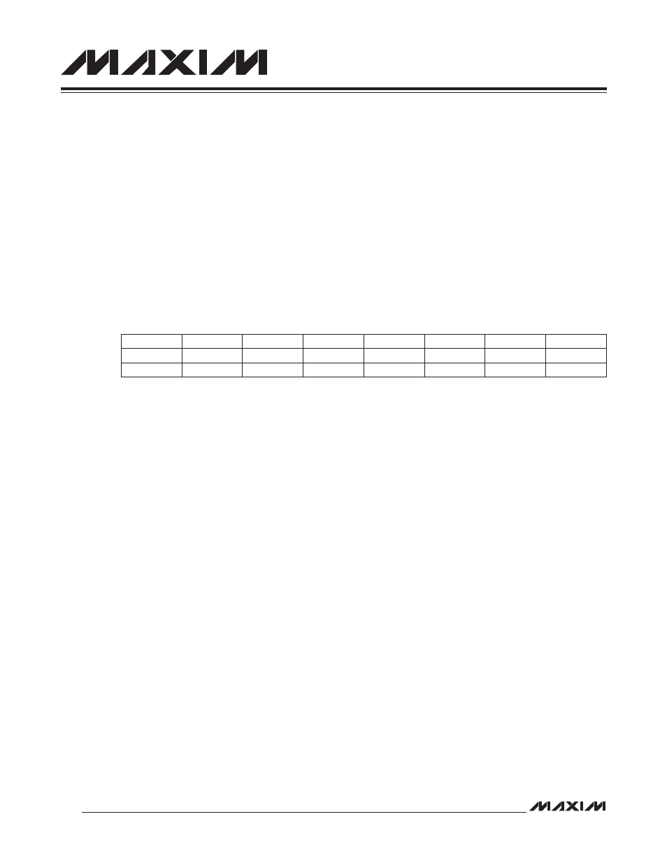
Bit #
7
6
5
4
3
2
1
0
Name
PCF4
PCF3
PCF2
PCF1
PCF0
SMO
OPM
DPE
Reset
0
0
0
0
0
0
0
0
Access
rw
rw
rw
rw
rw
rw
rw
rw