5 clock control register (i2cck, m3[0dh]), 5 clock control register (i2cck, m3[0dh]) -5, Maxq family user’s guide: maxq2010 supplement – Maxim Integrated MAXQ Family Users Guide: MAXQ2010 Supplement User Manual
Page 128

MAXQ Family User’s Guide:
MAXQ2010 Supplement
22-5
Note that this bit has no effect when the I
2
C is operating in slave mode (I2CMST = 0) and is reset to 0 when I2CMST
= 0 or I2CEN = 0. Also, the I2CSTART and I2CSTOP are mutually exclusive. If both bits are set at the same time, it
is considered as an invalid operation and the I
2
C controller ignores the request and resets both bits to 0. Setting the
I2CSTART bit to 1 while I2CSTOP = 1 is an invalid operation and is ignored, leaving the I2CSTART bit cleared to 0.
Bit 5: I
2
C Data Acknowledge Bit (I2CACK). This bit selects the acknowledge bit returned by the I
2
C controller while
acting as a receiver. Setting this bit to 1 generates a NACK (leaving SDA high). Clearing the I2CACK bit to 0 generates
an ACK (pulling SDA low) during the acknowledgement cycle. This bit retains its value unless changed by software or
hardware. When an I
2
C abort is in progress (I2CRST = 1), this bit is set to 1 by hardware, and software writes to this
bit are ignored when I2CRST = 1.
Bit 4: I
2
C Clock Stretch Select (I2CSTRS). Setting this bit to 1 enables clock stretching after the falling edge of the
8th clock cycle. Clearing this bit to 0 enables clock stretching after the falling edge of the 9th clock cycle. This bit has
no effect when clock stretching is disabled (I2CSTREN = 0).
Bit 2: I
2
C Transfer Mode (I2CMODE). The transfer mode bit selects the direction of data transfer with respect to the
master. When the I2CMODE bit is set to 1, the master is operating in receiver mode (reading from slave). When the
I2CMODE bit is cleared to 0, the master is operating in transmitter mode (writing to slave).
Note that software writing to this bit is prohibited in slave mode. When operating in master mode, software configures
this bit to the desired direction of data transfer. When operating in slave mode, the direction of data transfer is deter-
mined by the RW bit received during the address stage, and this bit reflects the actual R//W bit value in the current
transfer and is set by hardware. Software writing to this bit in slave mode is ignored.
Bit 1: I
2
C Master-Mode Enable (I2CMST). The I2CMST bit functions as a master-mode enable bit for the I
2
C mod-
ule. When the I2CMST bit is set to 1, the I
2
C operates as a master. When the I2CMST is cleared to 0, the I
2
C module
operates in slave mode. This bit is automatically cleared whenever the I
2
C controller receives a slave address match
(I2CAMI = 1), loses arbitration (I2CALI = 1), or receives a general call address (I2CGCI = 1, I2CGCEN = 1).
Bit 0: I
2
C Enable (I2CEN). This bit enables the I
2
C function. When set to 1, the I
2
C communication unit is enabled.
When cleared to 0, the I
2
C function is disabled.
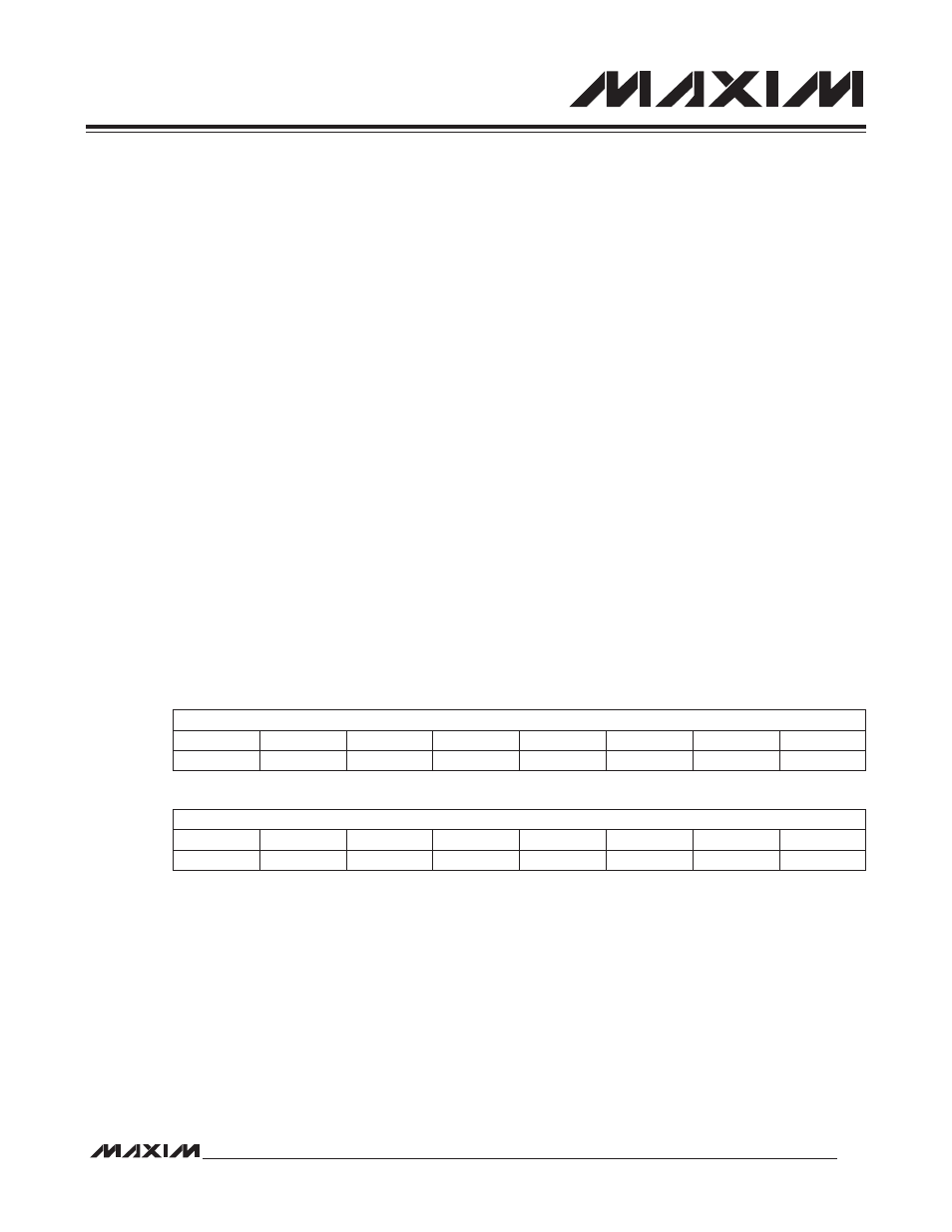
22.1.5 Clock Control Register (I2CCK, M3[0Dh])
Bits 15:8: I
2
C Clock High (I2CCKH[7:0]). These bits define the I
2
C SCL high period in number of system clock, with
bit 7 as the most significant bit. The duration of SCL high time is calculated using the following equation:
I
2
C High Time Period = System Clock x (I2CCKH[7:0] + 1)
When operating in master mode, I2CCKH must be set to a minimum value of 2 to ensure proper operation. Any value
less than 2 is set to 2.
Note 1: Write to this register is ignored when I2CBUSY = 0.
Note 2: This register has no function in slave mode.
Bit #
15
14
13
12
11
10
9
8
Name
I2CCKH
Reset
0
0
0
0
0
0
1
0
Access
rw
rw
rw
rw
rw
rw
rw
rw
Bit #
7
6
5
4
3
2
1
0
Name
I2CCKL
Reset
0
0
0
0
0
1
0
0
Access
rw
rw
rw
rw
rw
rw
rw
rw
