Hardware testpoints, Chapter 6 troubleshooting, Figure 6.11 main control board test points – Rockwell Automation 1336T FORCE Series B User Manual
Page 246: Tb10, J3 j4, Tb11, Testpoint application, Testpoint, Application
Chapter 6
Troubleshooting
6–34
Hardware Testpoints
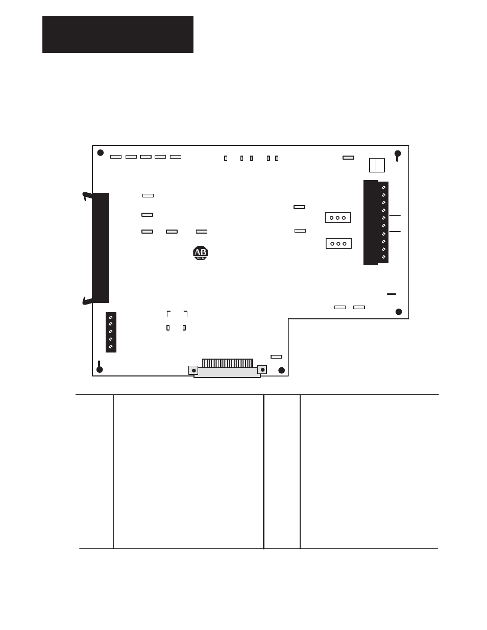
The Hardware Testpoints on the Series B 1336 FORCE Control Board are
illustrated in Figure 6.11. The accompanying table details the expected
output from each testpoint.
Figure 6.11
Main Control Board Test Points
Base
Driver
Board
Control
Signals
J7
TE
1
Drive to
Drive
Interface
J5
SHUNT +
Adapter Board Interface
+15V
TB10
D1
TP1
10
D2
D3
D5
VP Indicator
TP2 TP3
TP5
TP4
AGND –15V
+5V
DGND
D4
Enable
SHUNT –
SHIELD
ENC A
ENC A
ENC B
ENC B
ENC +
ENC –
SHIELD
TP24
TP23
12V ISO ISO COM
TP8
J1
V –
C_L
J3
J4
5V
12V
5V
12V
Encoder Feedback
(J3 & J4 must be set
for same voltage)
CP Indicator
TP1
TP2
TP3
TP4
TP5
TP6
TP7
TP8
TP9
TP10
TP11
TP12
TP13
TP14
TP15
DGND
+5V
+15V
AGND
–15V
–2.5 to 2.5 V
0 to 2.5V
+5V when faulted
CHA Encoder Fdbk 0 to 5 Square Wave with respect
to TP1 or TP25 DGND
Test DAC2 (Development Use Only)
Square Wave (Follows Carrier Frequency)
Test DAC1 (Development Use Only)
CHB Encoder Fdbk 0 to 5V Square Wave with respect to
TP1 or TP25 DGND
Bus Voltage FDBK (4V = 650 vdc)
Feed Forward Voltage (0 to +/– 7.5V sine wave)
Flt Trp
1
2 3
1
2 3
SHD
TB11
C_H
V+
D43
D47
TP25
STS PWR
D2D
DGND
TP13
TP9
TP14
DC Bus
FDBK
TP16
TP17
I
A
FDBK
I
c
FDBK
TP18
I
q
CMD
TP19
I
d
CMD
Testpoint
Application
TP16
TP17
TP18
TP19
TP20
TP21
TP22
TP23
TP24
TP25
Testpoint
Ia FDBK (0 to =/– 5V sine wave) same as Iq feedback
Ic FDBK (0 to =/– 5V sine wave) same as Iq feedback
Iqs Command (0 to +/– 10V sine wave)
Ids Command (0 to +/– 10V sine wave)
Master Reset (5V = Reset)
Id FDBK (0 to +/– 5V sine wave)
Feed Forward Voltage (0 to +/–/7.5V sine wave)
ISO 12V for Tachometer/Encoder
ISO RTN for Tachometer/Encoder
DGND
Application