Figure 4-2, Boot block a, Functional description – Artesyn CPCI-6200 Installation and Use (May 2015) User Manual
Page 88
Functional Description
CPCI-6200 Installation and Use (6806800J66E)
88
A hardware flash bank write protect switch is provided on the CPCI-6200 to enable write
protection of the NOR flash. Regardless of the state of the software flash write protect bit in the
NOR Flash Control/Status register, write protection is enabled when this switch is ON. When
this switch is OFF, write protection is controlled by the state of the software flash write protect
bits and can only be disabled by clearing this bit in the NOR FLASH Control/Status register. Note
that the F_WE_HW bit reflects the state of the switch and is only software readable whereas
the F_WP_SW bit supports both read and write operations.
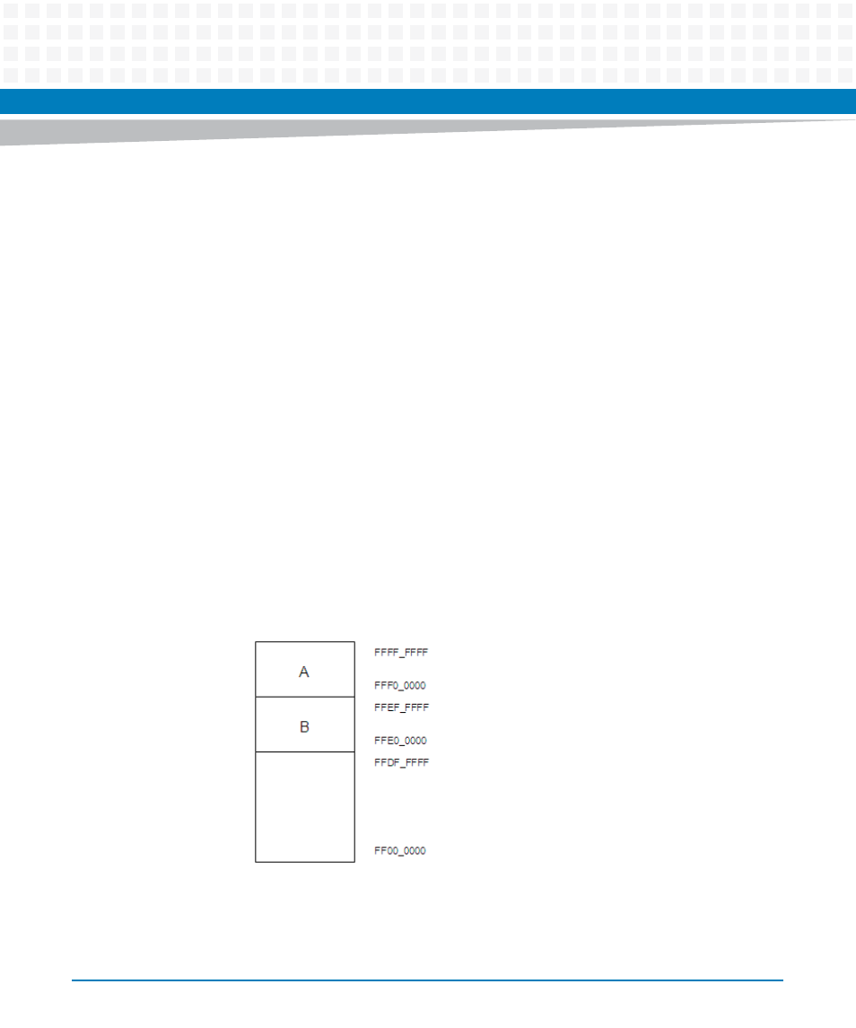
CPCI-6200 provides a dual boot option. You can boot from one of two separate boot images in
the boot flash bank called boot block A and boot block B. Boot blocks A and B are both 1 MB in
size and are located at the top (highest address) 2 MB of the boot flash memory space. Boot
block A is located at the highest 1 MB block, while boot block B is in the next highest 1 MB
block. A flash boot block switch is used to select between block A and block B. When the switch
is OFF, the flash memory map is normal and block A is selected. When the switch is ON, block
B is mapped to the highest address. The MAP_SELECT bit in the Flash Control/Status register
can disable the jumper and restore the memory map to the normal configuration where block
A is selected.
For additional information, see
NOR Flash Control and Status Register
and
Figure 4-2
Boot Block A