4 system i/o memory map, Table 8-4, System i/o memory map – Artesyn CPCI-6200 Installation and Use (May 2015) User Manual
Page 188
Memory Maps and Addresses
CPCI-6200 Installation and Use (6806800J66E)
188
8.4
System I/O Memory Map
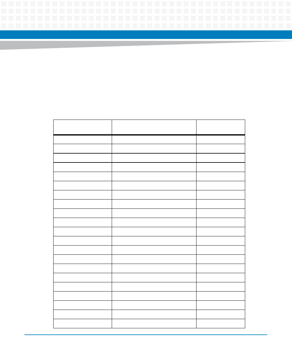
System resources, including system control and status registers, external timers, flash, and
DUART, are mapped to a 224 MB address range that is accessible from the CPCI-6200 local bus
via the MPC8572 LBC. The memory map is defined in the following table including the LBC
bank chip select used to decode the register.
Table 8-4 System I/O Memory Map
Address
Definition
LBC Bank/Chip
Select
F200 0000
3
System Status Register
3
F200 0001
3
System Control Register
3
F200 0002
3
FP LEDs Control & Status Register
3
F200 0003
3
NOR Flash Control/Status Register
3
F200 0004
3
Interrupt Register 1
3
F200 0005
3
Interrupt Register 2
3
F200 0006
3
Interrupt Mask Register
3
F200 0007
1
Reserved
3
F200 0008
3
Presence Detect Register
3
F200 0009–F200 000F
1
Reserved
3
F200 0010
3
Nand Flash Chip 1 Control Register
3
F200 0011
3
Nand Flash Chip 1 Select Register
3
F200 0012
3
Nand Flash Chip 1 Presence Register
3
F200 0013
3
Nand Flash Chip 1 Status Register
3
F200 0014
3
Nand Flash Chip 2 Control Register
3
F200 0015
3
Nand Flash Chip 2 Select Register
3
F200 0016
3
Nand Flash Chip 2 Presence Register
3
F200 0017
3
Nand Flash Chip 2 Status Register
3
F200 0018
3
CPCI Control & Status Register
3
F200 0019
3
Geographic Address Read Register
3
F200 001A–F200 001F
1
Reserved
3