2 cpci-6200 memory map, Table 8-2, Cpci-6200 address memory map – Artesyn CPCI-6200 Installation and Use (May 2015) User Manual
Page 186: Figure 8-1, Cpci-6200 memory map diagram
Memory Maps and Addresses
CPCI-6200 Installation and Use (6806800J66E)
186
8.2
CPCI-6200 Memory Map
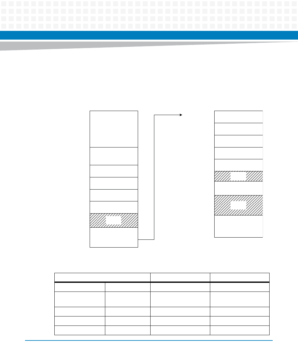
The following diagram and the succeeding table detail the physical memory map
implemented by the MotLoad firmware.
Figure 8-1
CPCI-6200 Memory Map Diagram
Table 8-2 CPCI-6200 Address Memory Map
Processor Address
Size
Definition
Start
End
0x0_0000_0000
top_dram - 1
dram_size (3.5 GB max)
System Memory (DDR3
SO-DIMMs)
0x0_E000_0000
0x0_EFF_FFFF
256 MB
PCI 0 Memory Space
0x0_F000_0000
0x0_F07F_FFFF
8 MB
PCI 0 I/O Space
0x0_F080_0000
0x0_F0BF_FFFF
4 MB
PCI 1 Memory Space
0x0_0000_0000
PCI Memory 0
(256 MB)
System Memory
(3.5 GB)
Reserved
(15 MB)
PCI I/O 0
(8 MB)
PCI Memory 1
(4 MB)
PCI I/O 1
(4 MB)
CPU Internal Register
(1 MB)
LBC
(224 MB)
Board Registers
(64 KB) CS3
Dual UART
(64 KB) CS4
32-bit Timers
(64 KB) CS5
NAND Flash 1
(32 KB) CS1
NAND Flash 2
(32 KB) CS1
Reserved
(3.75 MB)
MRAM
(512 KB) CS2
Reserved
(91.5 MB)
Flash A
(128 MB) CS0
0x0_DFFF_FFFF
0x0_E000_0000
0x0_EFFF_FFFF
0x0_E000_0000
0x0_F07F_FFFF
0x0_F080_0000
0x0_F0BF_FFFF
0x0_F0C0_0000
0x0_F0FF_FFFF
0x0_F100_0000
0x0_F10F_FFFF
0x0_F110_0000
0x0_F1FF_FFFF
0x0_F200_0000
0x0_FFFF_FFFF
0x0_F200_FFFF
0x0_F201_0000
0x0_F200_0000
0x0_F201_FFFF
0x0_F202_0000
0x0_F202_FFFF
0x0_F203_0000
0x0_F203_7FFF
0x0_F203_8000
0x0_F203_FFFF
0x0_F204_0000
0x0_F23F_FFFF
0x0_F240_0000
0x0_F7FF_FFFF
0x0_F800_0000
0x0_FFFF_FFFF
0x0_F247_FFFF
0x0_F248_0000