Clock resources, Global clock network sources, Clock resources -2 – Altera MAX 10 Clocking and PLL User Manual
Page 8: Global clock network sources -2
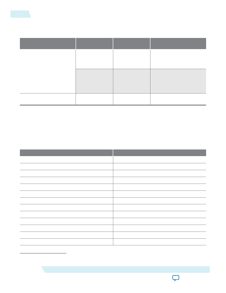
Clock Resources
Table 2-1: MAX 10 Clock Resources
Clock Resource
Device
Number of Resources
Available
Source of Clock Resource
Dedicated clock input pins
• 10M02
• 10M04
• 10M08
8 single-ended or 4
differential
CLK[3..0][p,n]
pins on the
left and right of the I/O
banks
• 10M16
• 10M25
• 10M40
• 10M50
16 single-ended or 8
differential
CLK[7..0][p,n]
pins on the
top, left, bottom, and right of
the I/O banks
DPCLK
pins
All
4
DPCLK[3..0]
pins on the left
and right of the I/O banks
For more information about the clock input pins connections, refer to the pin connection guidelines.
Related Information
Global Clock Network Sources
Table 2-2: MAX 10 Clock Pins Connectivity to the GCLK Networks
CLK
Pin
GCLK
CLK0p
GCLK[0,2,4]
CLK0n
GCLK[1,2]
CLK1p
GCLK[1,3,4]
CLK1n
GCLK[0,3]
CLK2p
GCLK[5,7,9]
CLK2n
GCLK[6,7]
CLK3p
GCLK[6,8,9]
CLK3n
GCLK[5,8]
CLK4p
(1)
GCLK[10,12,14]
CLK4n
(1)
GCLK[11,12]
CLK5p
(1)
GCLK[11,13,14]
CLK5n
(1)
GCLK[10,13]
CLK6p
(1)
GCLK[15,17,19]
(1)
This only applies to 10M16, 10M25, 10M40, and 10M50 devices.
2-2
Clock Resources
UG-M10CLKPLL
2015.05.04
Altera Corporation
MAX 10 Clocking and PLL Architecture and Features