Global clock control block, Global clock control block -4 – Altera MAX 10 Clocking and PLL User Manual
Page 10
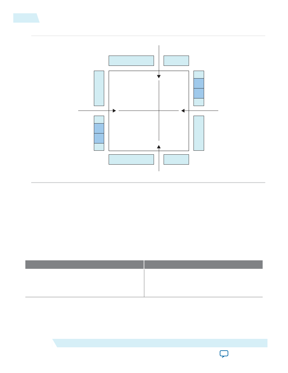
Figure 2-2: GCLK Network Sources for 10M16, 10M25, 10M40, and 10M50 Devices
DPCLK2
DPCLK3
DPCLK0
DPCLK1
CLK[0,1][p,n]
CLK[2,3][p,n]
GCLK[0..4]
GCLK[5..9]
CLK[4,5][p,n]
CLK[6,7][p,n]
GCLK[15..19]
GCLK[10..14]
Global Clock Control Block
The clock control block drives GCLKs. The clock control blocks are located on each side of the device,
close to the dedicated clock input pins. GCLKs are optimized for minimum clock skew and delay.
The clock control block has the following functions:
• Dynamic GCLK clock source selection (not applicable for
DPCLK
pins and internal logic input)
• GCLK multiplexing
• GCLK network power down (dynamic enable and disable)
Table 2-3: Clock Control Block Inputs
Input
Description
Dedicated clock input pins
Dedicated clock input pins can drive clocks or
global signals, such as synchronous and asynchro‐
nous clears, presets, or clock enables onto given
GCLKs.
2-4
Global Clock Control Block
UG-M10CLKPLL
2015.05.04
Altera Corporation
MAX 10 Clocking and PLL Architecture and Features