Pll features, Pll locations, Pll features -10 – Altera MAX 10 Clocking and PLL User Manual
Page 16: Pll locations -10
PLL Features
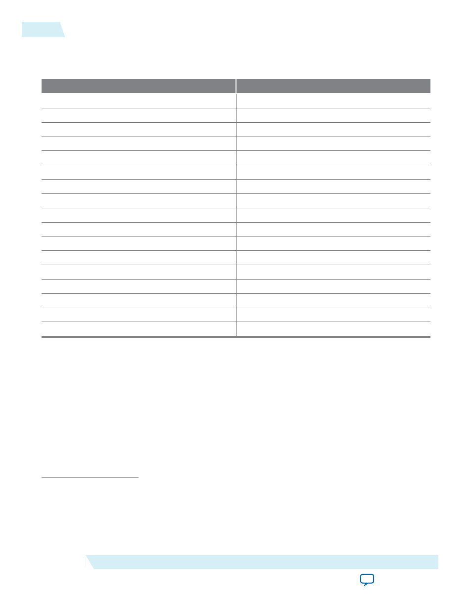
Table 2-4: MAX 10 PLL Features
Feature
Support
C
output counters
5
M
,
N
,
C
counter sizes
1 to 512
(2)
Dedicated clock outputs
1 single-ended or 1 differential
Dedicated clock input pins
4 single-ended or 2 differential
Spread-spectrum input clock tracking
Yes
(3)
PLL cascading
Through GCLK
Source synchronous compensation
Yes
No compensation mode
Yes
Normal compensation
Yes
Zero-delay buffer compensation
Yes
Phase shift resolution
Down to 96 ps increments
(4)
Programmable duty cycle
Yes
Output counter cascading
Yes
Input clock switchover
Yes
User mode reconfiguration
Yes
Loss of lock detection
Yes
4:1 multiplexer
CLK
input selection
Yes
PLL Locations
The following figures show the physical locations of the PLLs. Every index represents one PLL in the
device. The physical locations of the PLLs correspond to the coordinates in the Quartus II Chip Planner.
(2)
C
counters range from 1 through 512 if the output clock uses a 50% duty cycle. For any output clocks using a
non-50% duty cycle, the post-scale counters range from 1 through 256.
(3)
Only applicable if the input clock jitter is in the input jitter tolerance specifications.
(4)
The smallest phase shift is determined by the VCO period divided by eight. For degree increments, the
MAX 10 device family can shift all output frequencies in increments of at least 45°. Smaller degree
increments are possible depending on the frequency and divide parameters.
2-10
PLL Features
UG-M10CLKPLL
2015.05.04
Altera Corporation
MAX 10 Clocking and PLL Architecture and Features