Charge pump and loop filter – Altera MAX 10 Clocking and PLL User Manual
Page 51
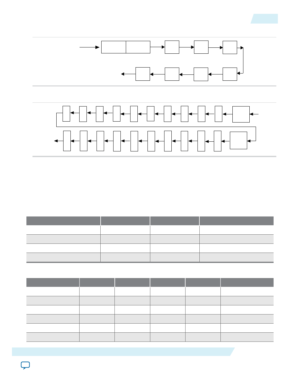
Figure 4-7: PLL Component Scan Chain Order
DATAIN
C1
C2
C3
C4
DATAOUT
MSB
LF
CP
LSB
N
M
C0
Figure 4-8: PLL Post-Scale Counter Scan Chain Bit Order
DATAIN
rbypass
HB
7
HB
6
HB
5
HB
4
HB
3
HB
2
HB
1
HB
0
rselodd
LB
7
LB
6
LB
5
LB
4
LB
3
LB
2
LB
1
LB
0
DATAOUT
HB
9
HB
8
LB
9
LB
8
Charge Pump and Loop Filter
You can reconfigure the following settings to update the PLL bandwidth in real time:
• Charge pump (I
CP
)
• Loop filter resistor (R)
• Loop filter capacitor (C)
Table 4-2: Charge Pump Bit Control
CP[2]
CP[1]
CP[0]
Setting (Decimal)
0
0
0
0
0
0
1
1
0
1
1
3
1
1
1
7
Table 4-3: Loop Filter Resistor Value Control
LFR[4]
LFR[3]
LFR[2]
LFR[1]
LFR[0]
Setting (Decimal)
0
0
0
0
0
0
0
0
0
1
1
3
0
0
1
0
0
4
0
1
0
0
0
8
1
0
0
0
0
16
1
0
0
1
1
19
UG-M10CLKPLL
2015.05.04
Charge Pump and Loop Filter
4-13
MAX 10 Clocking and PLL Implementation Guides
Altera Corporation
See also other documents in the category Altera Measuring instruments:
- MAX 10 JTAG (15 pages)
- MAX 10 Power (21 pages)
- Unique Chip ID (12 pages)
- Remote Update IP Core (43 pages)
- Device-Specific Power Delivery Network (28 pages)
- Device-Specific Power Delivery Network (32 pages)
- Hybrid Memory Cube Controller (69 pages)
- ALTDQ_DQS IP (117 pages)
- MAX 10 Embedded Memory (71 pages)
- MAX 10 Embedded Multipliers (37 pages)
- MAX 10 FPGA (26 pages)
- MAX 10 FPGA (56 pages)
- USB-Blaster II (22 pages)
- GPIO (22 pages)
- LVDS SERDES (27 pages)
- User Flash Memory (33 pages)
- ALTDQ_DQS2 (100 pages)
- Avalon Tri-State Conduit Components (18 pages)
- Cyclone V Avalon-MM (166 pages)
- Cyclone III FPGA Starter Kit (36 pages)
- Cyclone V Avalon-ST (248 pages)
- Stratix V Avalon-ST (286 pages)
- Stratix V Avalon-ST (293 pages)
- DDR3 SDRAM High-Performance Controller and ALTMEMPHY IP (10 pages)
- Arria 10 Avalon-ST (275 pages)
- Avalon Verification IP Suite (224 pages)
- Avalon Verification IP Suite (178 pages)
- FFT MegaCore Function (50 pages)
- DDR2 SDRAM High-Performance Controllers and ALTMEMPHY IP (140 pages)
- Floating-Point (157 pages)
- Integer Arithmetic IP (157 pages)
- Embedded Peripherals IP (336 pages)
- JESD204B IP (158 pages)
- Low Latency Ethernet 10G MAC (109 pages)
- LVDS SERDES Transmitter / Receiver (72 pages)
- Nios II Embedded Evaluation Kit Cyclone III Edition (3 pages)
- Nios II Embedded Evaluation Kit Cyclone III Edition (80 pages)
- IP Compiler for PCI Express (372 pages)
- Parallel Flash Loader IP (57 pages)
- Nios II C2H Compiler (138 pages)
- RAM-Based Shift Register (26 pages)
- RAM Initializer (36 pages)
- Phase-Locked Loop Reconfiguration IP Core (51 pages)
- DCFIFO (28 pages)