Source synchronous mode, No compensation mode – Altera MAX 10 Clocking and PLL User Manual
Page 21
Source Synchronous Mode
If the data and clock arrive at the same time at the input pins, the phase relationship between the data and
clock remains the same at the data and clock ports of any I/O element input register.
You can use this mode for source synchronous data transfers. Data and clock signals at the I/O element
experience similar buffer delays as long as both signals use the same I/O standard.
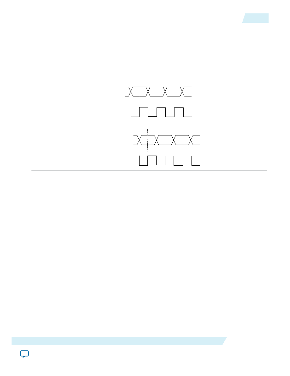
Figure 2-12: Example of Phase Relationship Between Clock and Data in Source Synchronous Mode
Data pin
PLL reference
clock at input pin
Data at register
Clock at register
Source synchronous mode compensates for clock network delay, including any difference in delay
between the following two paths:
• Data pin to I/O element register input
• Clock input pin to the PLL PFD input
For all data pins clocked by a source synchronous mode PLL, set the input pin to the register delay chain
in the I/O element to zero in the Quartus II software. All data pins must use the PLL COMPENSATED
logic option in the Quartus II software.
No Compensation Mode
In no compensation mode, the PLL does not compensate for any clock networks. This mode provides
better jitter performance because clock feedback into the PFD does not pass through as much circuitry.
Both the PLL internal and external clock outputs are phase-shifted with respect to the PLL clock input.
UG-M10CLKPLL
2015.05.04
Source Synchronous Mode
2-15
MAX 10 Clocking and PLL Architecture and Features
Altera Corporation