Altera MAX 10 Clocking and PLL User Manual
Page 29
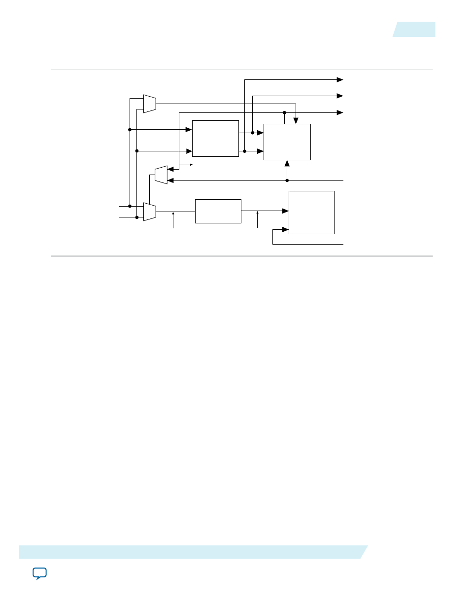
Figure 2-20: Automatic Clock Switchover Circuit Block Diagram
This figure shows a block diagram of the automatic switchover circuit built into the PLL.
Switchover
State
Machine
Clock
Sense
N Counter
PFD
clkswitch
(Provides Manual
Switchover Support)
activeclock
clkbad1
clkbad0
muxout
inclk0
inclk1
refclk
fbclk
clksw
When the current reference clock is not present, the clock sense block automatically switches to the
backup clock for PLL reference. You can select a clock source at the backup clock by connecting it to the
inclk1
port of the PLL in your design.
The clock switchover circuit also sends out three status signals—
clkbad[0]
,
clkbad[1]
, and
activeclock
—from the PLL to implement a custom switchover circuit in the logic array.
In automatic switchover mode, the
clkbad[0]
and
clkbad[1]
signals indicate the status of the two clock
inputs. When the
clkbad[0]
and
clkbad[1]
signals are asserted, the clock sense block detects that the
corresponding clock input has stopped toggling. These two signals are not valid if the frequency difference
between
inclk0
and
inclk1
is greater than 20%.
The
activeclock
signal indicates which of the two clock inputs (
inclk0
or
inclk1
) is selected as the
reference clock to the PLL. When the frequency difference between the two clock inputs is more than
20%, the
activeclock
signal is the only valid status signal.
Note: Glitches in the input clock may cause the frequency difference between the input clocks to be more
than 20%.
When the current reference clock to the PLL stops toggling, use the switchover circuitry to automatically
switch from
inclk0
to
inclk1
that runs at the same frequency. This automatic switchover can switch
back and forth between the
inclk0
and
inclk1
clocks any number of times when one of the two clocks
fails and the other clock is available.
For example, in applications that require a redundant clock with the same frequency as the reference
clock, the switchover state machine generates a signal (
clksw
) that controls the multiplexer select input.
In this case,
inclk1
becomes the reference clock for the PLL.
UG-M10CLKPLL
2015.05.04
Automatic Clock Switchover
2-23
MAX 10 Clocking and PLL Architecture and Features
Altera Corporation