Internal oscillator architecture and features, Plls architecture and features, Pll architecture – Altera MAX 10 Clocking and PLL User Manual
Page 14: Internal oscillator architecture and features -8, Plls architecture and features -8, Pll architecture -8
Related Information
•
Guideline: Clock Enable Signals
on page 3-1
•
on page 5-1
•
on page 5-2
Internal Oscillator Architecture and Features
MAX 10 devices have built-in internal ring oscillator with clock multiplexers and dividers. The internal
ring oscillator operates up to 232 MHz which is not accessible. This operating frequency further divides
down to slower frequencies.
By default internal oscillator is turned off in user mode. You can turn on the oscillator by asserting the
oscena
signal in the Internal Oscillator IP core.
When the
oscena
input signal is asserted, the oscillator is enabled and the output can be routed to the
logic array through the
clkout
output signal. When the
oscena
signal is set low, the
clkout
signal is
constant high. You can analyze this delay using the TimeQuest timing analyzer.
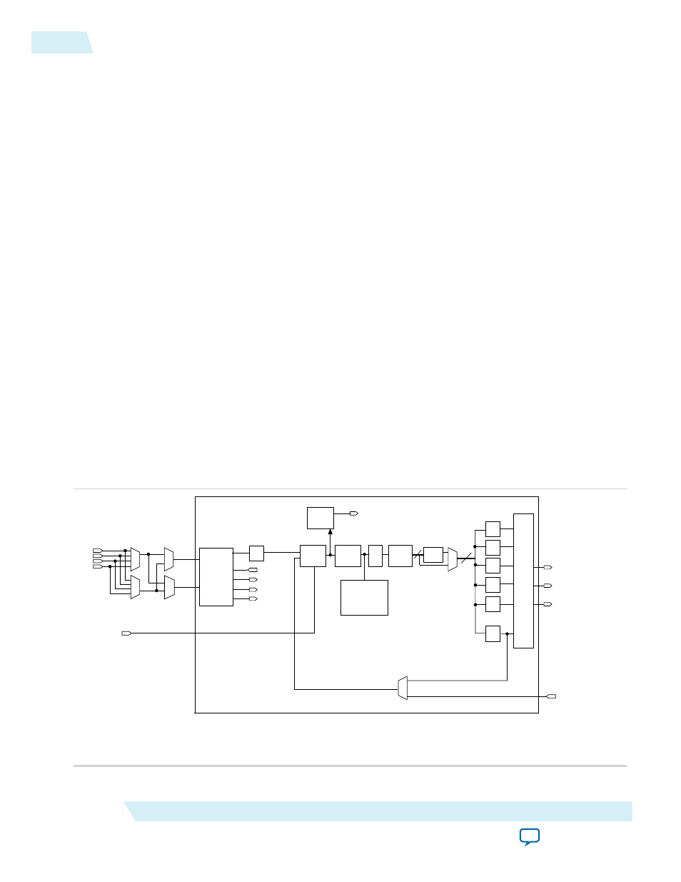
PLLs Architecture and Features
PLL Architecture
The main purpose of a PLL is to synchronize the phase and frequency of the voltage-controlled oscillator
(VCO) to an input reference clock.
Figure 2-7: MAX 10 PLL High-Level Block Diagram
Each clock source can come from any of the two or four clock pins located on the same side of the device
as the PLL.
Clock
Switchover
Block
inclk0
inclk1
pfdena
clkswitch
clkbad0
clkbad1
activeclock
PFD
LOCK
circuit
lock
÷n
CP
LF
VCO
÷2 (1)
÷C0
÷C1
÷C2
÷C3
÷C4
÷M
PLL
output
mux
GCLKs
ADC clock (2)
8
8
GCLK
networks
No Compensation; ZDB Mode
Source-Synchronous; Normal Mode
VCO
Range
Detector
Notes:
(1) This is the VCO post-scale counter K.
(2) Only counter C0 of PLL1 and PLL3 can drive the ADC clock.
PLL
External clock output
4:1
Multiplexer
4:1
Multiplexer
CLKIN
2-8
Internal Oscillator Architecture and Features
UG-M10CLKPLL
2015.05.04
Altera Corporation
MAX 10 Clocking and PLL Architecture and Features