Altera MAX 10 Clocking and PLL User Manual
Page 11
Input
Description
DPCLK
pins
DPCLK
pins are bidirectional dual function pins that
are used for high fan-out control signals, such as
protocol signals,
TRDY
and
IRDY
signals for PCI via
the GCLK. Clock control blocks that have inputs
driven by
DPCLK
pins cannot drive PLL inputs.
PLL counter outputs
PLL counter outputs can drive the GCLK.
Internal logic
You can drive the GCLK through logic array
routing to enable the internal logic elements (LEs)
to drive a high fan-out, low-skew signal path. Clock
control blocks that have inputs driven by internal
logic cannot drive PLL inputs.
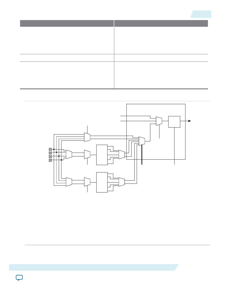
Figure 2-3: Clock Control Block
clkswitch (1)
Static Clock Select (3)
Static Clock
Select (3)
Internal Logic
Clock Control Block
DPCLK
clkselect[1..0] (2)
Internal Logic (4)
inclk1
inclk0
CLK[n + 3]
CLK[n + 2]
CLK[n + 1]
CLK[n]
fIN
C0
C1
C2
PLL
Global
Clock
Enable/
Disable
C3
C4
Notes:
(1) The clkswitch signal can either be set through the configuration file or dynamically set when using the manual PLL switchover
feature. The output of the multiplexer is the input clock (fIN) for the PLL.
(2) The clkselect[1..0] signals are fed by internal logic. You can use the clkselect[1..0] signals to dynamically select the clock source for
the GCLK when the device is in user mode. Only one PLL (applicable to PLLs on the same side) can be selected as the clock source to
the GCLK.
(3) The static clock select signals are set in the configuration file. Therefore, dynamic control when the device is in user mode is not
feasible.
(4) You can use internal logic to enable or disable the GCLK in user mode.
clkswitch (1)
inclk1
inclk0
fIN
C0
C1
C2
PLL
C3
C4
Each MAX 10 device has a maximum of 20 clock control blocks. There are five clock control blocks on
each side of the device.
UG-M10CLKPLL
2015.05.04
Global Clock Control Block
2-5
MAX 10 Clocking and PLL Architecture and Features
Altera Corporation