Programmable phase shift – Altera MAX 10 Clocking and PLL User Manual
Page 26
•
on page 4-13
Provides more information about the PLL components to update PLL bandwidth in real time.
•
Programmable Bandwidth Parameter Settings
Programmable Phase Shift
The MAX 10 devices use phase shift to implement clock delays. You can phase shift the output clocks
from the MAX 10 PLLs using one of the following methods:
• Fine resolution using VCO phase taps
• Coarse resolution using counter starting time
The VCO phase output and counter starting time are the most accurate methods of inserting delays.
These methods are purely based on counter settings, which are independent of process, voltage, and
temperature.
The MAX 10 devices support dynamic phase shifting of VCO phase taps only. The phase shift is configu‐
rable for any number of times. Each phase shift takes about one
scanclk
cycle, allowing you to implement
large phase shifts quickly.
Fine Resolution Phase Shift
Fine resolution phase shifts are implemented by allowing any of the output counters (
C[4..0]
) or the
M
counter to use any of the eight phases of the VCO as the reference clock. This allows you to adjust the
delay time with a fine resolution. The following equation shows the minimum delay time that you can
insert using this method.
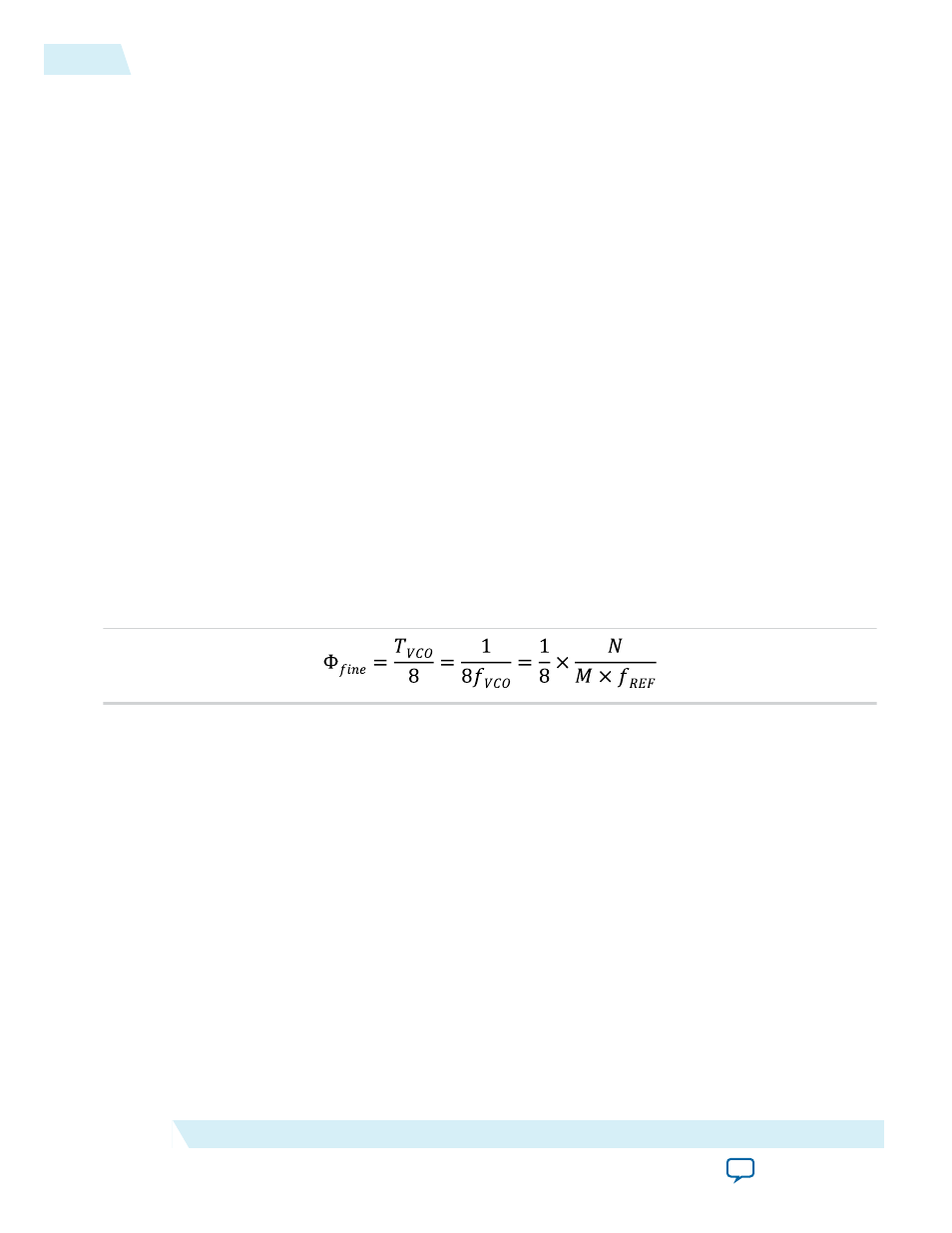
Figure 2-17: Fine Resolution Phase Shift Equation
f
REF
in this equation is the input reference clock frequency
For example, if f
REF
is 100 MHz,
N
= 1, and
M
= 8, then f
VCO
= 800 MHz, and Φ
fine
= 156.25 ps. The PLL
operating frequency defines this phase shift, a value that depends on the reference clock frequency and
counter settings.
The following figure shows an example of phase shift insertion using the fine resolution through VCO
phase taps method. The eight phases from the VCO are shown and labeled for reference.
2-20
Programmable Phase Shift
UG-M10CLKPLL
2015.05.04
Altera Corporation
MAX 10 Clocking and PLL Architecture and Features