Ds4830a user’s guide, Transmitting byte receiving byte, Transmitting slave address – Maxim Integrated DS4830A Optical Microcontroller User Manual
Page 86
DS4830A User’s Guide
86
to be set. Once set, writes to I2CBUF_M will be ignored. The first bit of data (most significant bit) will be shifted to
SDA when SCL is low. Each of the next seven bits will then be shifted following high to low transitions of SCL.
Following the 8
th
bit of data (least significant bit) being shifted to SDA, the SDA line will be released by the DS4830A
master controller. This allows the slave to signal an ACK or NACK during the 9
th
clock cycle. The DS4830A I
2
C
master controller samples the acknowledge bit following the 9
th
SCL rising edge. After the acknowledge bit is
sampled, the DS4830A I
2
C master controller will perform the following tasks:
• Set or clear the I2CNACKI flag to reflect the received acknowledge bit. The setting of I2CNACKI can
generate an interrupt if enabled.
• Set the I2CTXI flag to indicate that the I
2
C master controller transmit a complete byte. This can generate an
interrupt if enabled.
• Clear the I2CBUSY flag to indicate that the I
2
C master controller is not actively participating in the transfer of
data.
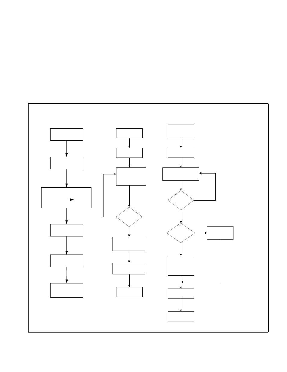
I2CNACKI =
ACKNOWLEDGE
Transmit I2CBUF_M[7:0]
I2CBUF_M[0] I2CMODE
I2CBUSY=1
I2CTXI=1
I2CBUSY=0
Write to
I2CBUF_M
RECEIVE
ACKNOWLEDGE
Transmitting
Byte
Receiving
Byte
I2CNACKI =
ACKNOWLEDGE
Transmit Shift
Register Byte,
MSB First
N
Y
I2CBUSY=1
8 Bits
Transmit?
I2CTXI=1
I2CBUSY=0
Write to
I2CBUF_M
Receive a Bit into
Shift Register
MSB first
N
Y
I2CBUSY=1
8 Bits
Received?
Load Shift
Register into
I2CBUF_M
I2CRXI=1
Send
I2CACK
Y
N
I2CROI=1
Receiver
Full
?
First SCL
Rising Edge
Generated
I2CBUSY=0
RECEIVE
ACKNOWLEDGE
Transmitting
Slave Address
Figure 10-5: Master I
2
C Data Flow