Ds4830a user’s guide, Program space, Data space (byte mode, cda0 = 0) – Maxim Integrated DS4830A Optical Microcontroller User Manual
Page 21: Data space (byte mode, cda0 = 1) executing from, Data space (word mode)

DS4830A User’s Guide
21
2.4.4.3 – Memory Map When Executing from SRAM
When executing from the SRAM:
• The utility ROM can be read as data, starting at 8000h of the data space. The utility ROM cannot be written.
• Reading of flash memory is executed normally. Writing to flash memory requires the use of the utility ROM
routines.
• One page (byte access mode) or both pages (word access mode) of the flash memory can be accessed as data
with an offset of 0000h. For byte access mode, the page of flash accessed is determined by the CDA0 bit.
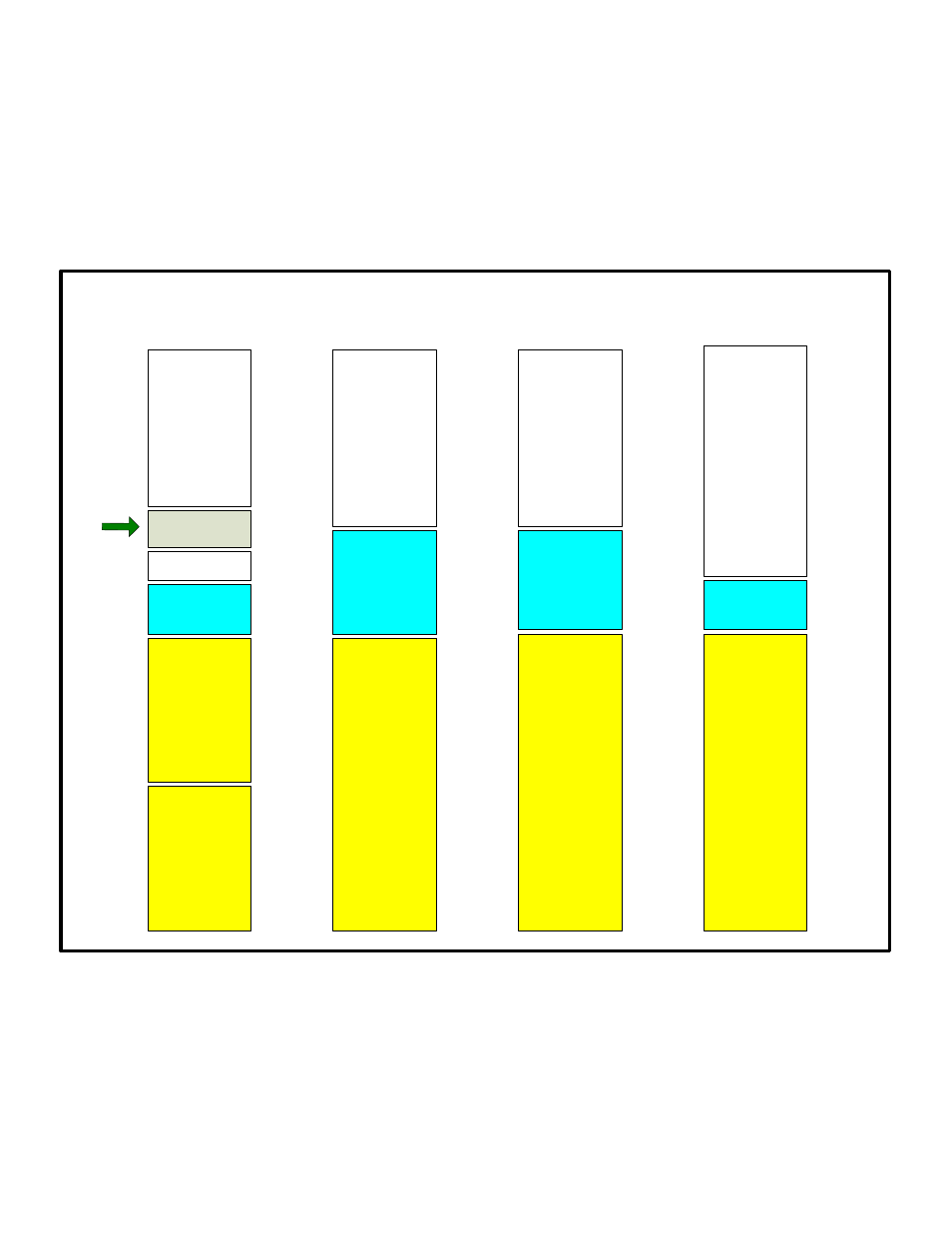
Figure 2-5 illustrates the mapping of the flash and utility ROM memory segments into data memory space when code is
executing from the SRAM memory segment.
2K * 16
SRAM
16K * 16
FLASH
(SEGMENT 0)
4K * 16
UTILITY ROM
PROGRAM
SPACE
16K * 16
FLASH
(SEGMENT 1)
0000h
3FFFh
4000h
7FFFh
8FFFh
A000h
A7FFh
FFFFh
8000h
32K * 8
LOWER HALF
(SEGMENT 0)
OF FLASH
DATA SPACE
(BYTE MODE,
CDA0 = 0)
0000h
FFFFh
8000h
32K * 8
UPPER HALF
(SEGMENT 1)
OF FLASH
0000h
FFFFh
DATA SPACE
(BYTE MODE,
CDA0 = 1)
EXECUTING FROM
32K * 16
FLASH
0000h
FFFFh
DATA SPACE
(WORD MODE)
8K * 8
UTILITY ROM
8K * 8
UTILITY ROM
4K * 16
UTILITY ROM
7FFFh
8000h
7FFFh
8000h
7FFFh
8FFFh
9FFFh
9FFFh
Figure 2-5: Memory Map When Executing from SRAM
