Ds4830a user’s guide – Maxim Integrated DS4830A Optical Microcontroller User Manual
Page 107
DS4830A User’s Guide
107
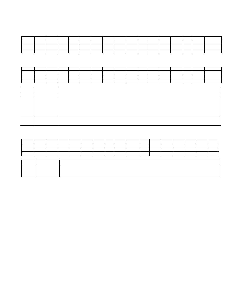
11.2.6 –
I
2
C
Slave Address Registers (I2CSLA_S, I2CSLA2_S, I2CSLA3_S and I2CSLA4_S)
I2CSLA_S
Bit
15
14
13
12
11
10
9
8
7
6
5
4
3
2
1
0
Name
-
-
-
-
-
-
-
-
A6
A5
A4
A3
A2
A1
A0
I2CMode
Reset*
0
0
0
0
0
0
0
0
0
0
1
1
0
1
1
0
Access
r
r
r
r
r
r
r
r
rw
rw
rw
rw
rw
rw
rw
rw
* Default value of I2CSLA_S is 36h.
I2CSLA2_S, I2CSLA3_S and I2CSLA4_S
Bit
15
14
13
12
11
10
9
8
7
6
5
4
3
2
1
0
Name
-
-
-
-
-
-
-
-
A6
A5
A4
A3
A2
A1
A0
I2CMode
Reset
0
0
0
0
0
0
0
0
0
0
0
0
0
0
0
0
Access
r
r
r
r
r
r
r
r
rw
rw
rw
rw
rw
rw
rw
rw
BIT
NAME
DESCRIPTION
15:8
Reserved
Reserved. The user should not write to these bits.
7:1
A[6:0]
I
2
C Slave Address. These address bits contain the address of the
I
2
C
slave interface. When a match to
this address is detected, the
I
2
C
controller automatically acknowledges the host with the I2CACK bit
value and the I2CAMI flag is set to ‘1’. An interrupt is generated if enabled. The I2CSLA_S is enabled by
default. Other slave address registers participate in the address match event only when the
corresponding slave address enable bit in the I2CCN_S register is set to ‘1’.
0
I2CMode
I
2
C Transfer Mode Select. This bit reflects the actual R/
W bit value in current value in
I
2
C
transfer and
set by hardware.
11.2.7 –
I
2
C
Slave Data Buffer Register (I2CBUF_S)
Bit
15
14
13
12
11
10
9
8
7
6
5
4
3
2
1
0
Name
D15
D14
D13
D12
D11
D10
D9
D8
D7
D6
D5
D4
D3
D2
D1
D0
Reset
0
0
0
0
0
0
0
0
0
0
0
0
0
0
0
0
Access
rw
rw
rw
rw
rw
rw
rw
rw
rw
rw
rw
rw
rw
rw
rw
rw
BIT
NAME
DESCRIPTION
15:0
D[15:0]
Data for
I
2
C
transfer is read from or written to this register. The
I
2
C
transmit and receive buffers are
different internal registers, however both are addressed at this register.
The receive FIFO and TX pages are read and written using the I2CBUF_S register.