Section 7 – analog-to-digital converter (adc), 1 – detailed description, 1 – adc controller – Maxim Integrated DS4830A Optical Microcontroller User Manual
Page 48: Ds4830a user’s guide
DS4830A User’s Guide
48
SECTION 7 – ANALOG-TO-DIGITAL CONVERTER (ADC)
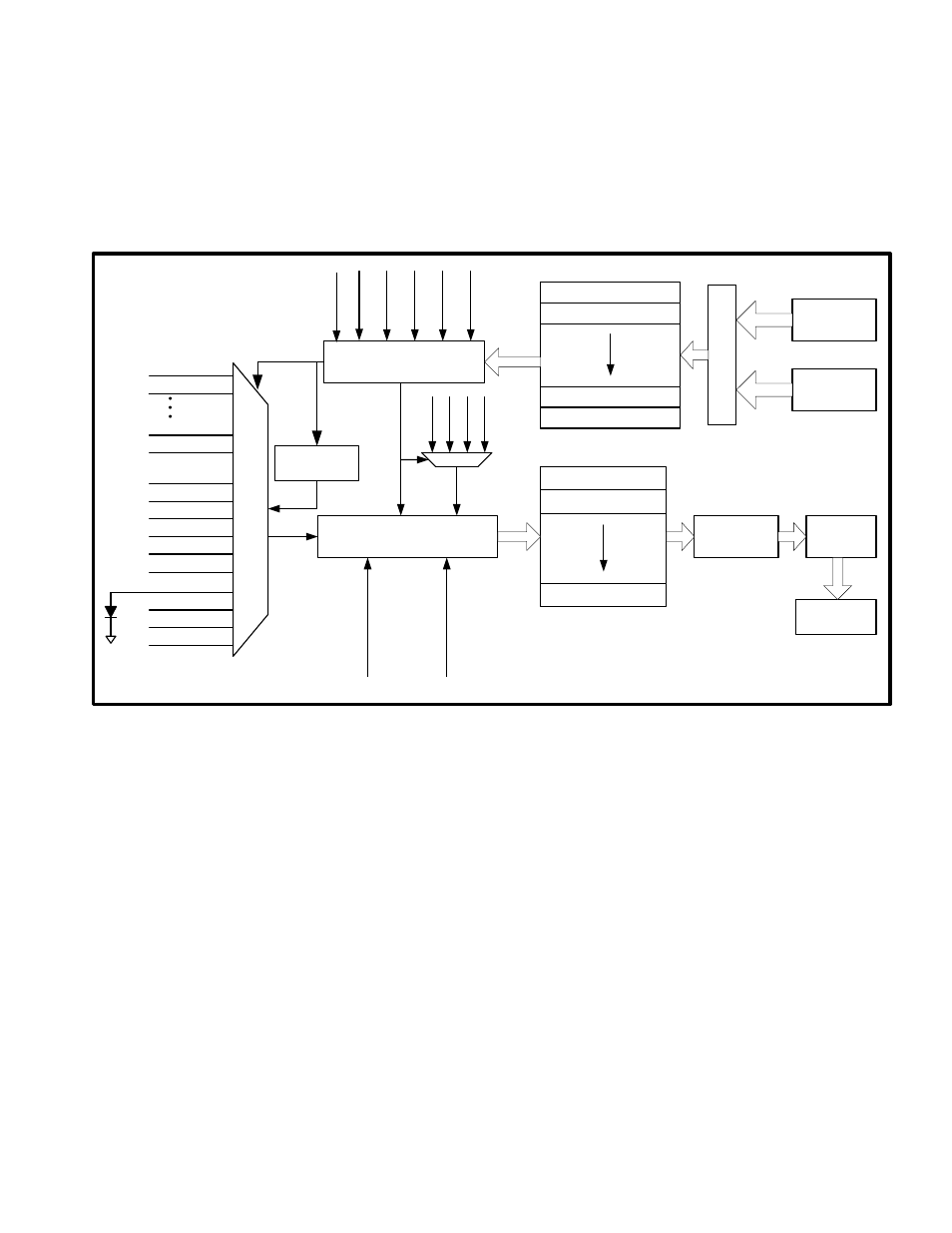
The DS4830A provides a 13-bit analog-to-digital converter (ADC) with 26-input MUX. As shown in Figure 7-1, the
MUX selects the ADC input from 16 external channels, DAC external references at REFINA and REFINB, V
DD
, DAC
Internal Reference, Internal Die Temperature, Sample and Hold at GP2-GP3 and GP12-GP13 and ADC Internal
Offset. The ADC external channels can operate in differential voltage mode or in single-ended voltage mode. An
internal channel is used exclusively to measure the die temperature. The REFINA and REFINB pins can be used as
analog channel independent to the DAC reference.
13-BIT ADC CORE
ADC-S0
ADC-S1
ADC-S14
ADC-S15
A
N
A
L
O
G
M
U
X
VOLTAGE OFFSET
(ADVOFF
)
INTERNAL DIE TEMP
Current Source
For Temperature
Measurement
ADC SEQUENCER
ADSTART
ADEND
ADCONV
ADCONT
ADCG
1
ADCG
4
ADGAIN
INTERNAL
REFERENCE
CONFIGURATION[0]
CONFIGURATION[19]
CONFIGURATION[1]
DATA BUFFER[0]
DATA BUFFER[24]
DATA BUFFER[1]
ADCFG=0
ADIDX[4:0]
READ
ADDATA
ADCG
3
ADCG
2
REFINA
REFINB
DAC INT REF
VDD
Reserved
Reserved
SH0
SH1
Internal Offset
NUM
_
SMP
CONFIGURATION[23]
DIGITAL
READOUT
ADCFG=1
ADIDX[4:0]
ADCAVG=1
ADIDX[4:0]
WRITE TO ADDATA
ADC SEQ
ADC AVG
REFAVG
Figure 7-1: ADC Functional Diagram
7.1 – Detailed Description
7.1.1 – ADC Controller
The ADC controller is the digital interface block between CPU and the ADC. It provides all necessary controls to the
ADC and the CPU interface. The ADC controller provides 25 buffers (0-24) for various configurations and data
buffers. By default, the ADC conversion result corresponding to each channel is placed in data buffers at the location
shown in Table 7-1. The user can override the default buffer locations and define alternate locations in the ADC Data
and Configuration register (ADDATA) during configuration by settling the LOC_OVR bit to ‘1’ in the ADC Control
register (ADCN). The internal temperature sensor and Sample and Hold (S/H) use fixed data buffer locations and
these locations should not be used for other channels if these peripherals are enabled. The ADC internal offset does
not have any data buffer and its measurement is performed with location override enable. Table 7-1 has the default
configuration and data buffer locations. The ADC controller provides various internal averaging options for individual
ADC channels, internal die temperature and S/H. See Section 7.1.9 for ADC Averaging.