4 – sample and hold conversion, 5 – adc frame sequence, 6 – adc reference – Maxim Integrated DS4830A Optical Microcontroller User Manual
Page 51

DS4830A User’s Guide
51
7.1.4 – Sample and Hold Conversion
The DS4830A has two Sample and Hold (S/H) inputs at pins GP2-GP3 and GP12-GP13. These can be
independently enabled or disabled by writing to their corresponding bit locations in the Sample and Hold Control
register (SHCN). See the Sample and Hold description in Section 8. The Sample and Hold uses data buffer 23 and
24 for S/H0 and S/H1 respectively. The Sample and Hold conversion complete flags are located in the ADST
register. When enabled with voltage conversions, the sample and hold conversions get time slots in between each
voltage conversion. See Figure 7-3, ADC Frame Sequence for more details.
7.1.5 – ADC Frame Sequence
When all modes (voltage, temperature, and sample and hold) are used simultaneously, the ADC controller uses time
slicing. The ADC controller uses the ADC sequence of voltage conversions as “primary channels” and sample and
hold as secondary channels. The time slicing rules are
1. The primary channels (ADC voltage channels) have priority over the secondary channels (S/Hs).
2. S/H0 has priority over S/H1 if both S/Hs are ready for conversion. However, in next slot for S/H, the S/H1 will
get slot even if S/H0 is also ready.
3. The internal die temperature gets the conversion slots at the end of ADC sequence.
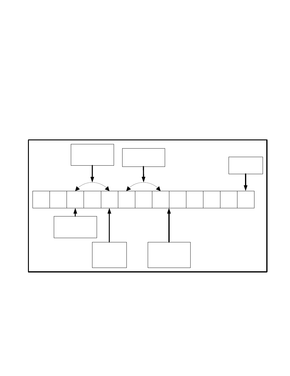
For example, if the ADC sequence mode conversion is enabled for channel 0, 4, 5, 6, both S/Hs and internal die
temperature are enabled and ready for conversion then the sequence of conversion is performed as shown in Figure
7-3.
CH0
CH4
S/H1
CH5
S/H0
CH6
Int
Temp
CH0
S/H1
CH4
……..
……..
Every alternate
channel is primary
channel
Both S/H0 & S/H1
are ready. S/H0
gets priority over
S/H1
S/H1 gets
chance here
even if S/H0
is ready.
Sequence
keeps
repeating
SH0 or 1 if
triggered by
internal or
SHEN0/1l
S/H0
End of Sequence.
Internal
Temperature gets
chance here.
Figure 7-3: ADC Frame Sequence
Notes:
1. Both Sample and Hold channels can occur simultaneously as they have dedicated resources.
2. Averaging is disabled.
7.1.6 – ADC Reference
The ADC has a 1.2V internal reference that must be enabled before the start of ADC conversion sequence. The
ADC controller provides INT_REF bit in the REFAVG register to control the ADC internal reference. By setting this bit
to ‘1’, the internal reference is enabled. The ADC internal reference needs approximate 1ms of stabilization time. The
ADC conversion should be started only after this stabilization time.
The ADC controller provides an option to bring out the ADC internal reference at GP1 pin (PIN6, Port2.1). By setting
REF_OUT bit in the REFAVG register and the bit 1 of the PINSEL register, the ADC internal reference is brought out
at GP1 pin.
