4 – pin capacitance discharge, Ds4830a user’s guide, Sample pulse width with external clock – Maxim Integrated DS4830A Optical Microcontroller User Manual
Page 68

DS4830A User’s Guide
68
SHEN0/1
or
INT_REIG0/1
Sample Pulse
Sample Pulse Width with external clock
CLKIN
….
Falling edge (Sample stop) depends
upon SSC[3:0]
300ns
min
….
….
SSC[3:0] = 0
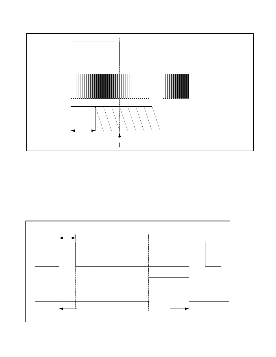
Figure 8-5: Sample Pulse Width with the External Clock
As shown in Figure 8-5, the sample pulse width time depends upon the SSC bits value when the external clock is
selected (CLK_SEL = 1).
8.1.4 – Pin Capacitance Discharge
Before the sample and hold circuitry start sampling, the DS4830A has an option to discharge pin capacitance. The
SHCN register has PIN_DIS0 and PIN_DIS1 bits to enable the pin discharge function before sampling begins. This
is an optional feature, which generates a discharge pulse that discharges the pin or PCB capacitance for the sample
and hold channels. The discharge pulse is active after the corresponding sample and hold channel’s conversion is
complete and goes inactive on the rising edge of SHEN0 or SHEN1 pulse. See pin discharge timing is shown in
Figure 8-6.
Sample Time
(min 300nSec)
Conversion Time
Pin discharge function
Pin Discharge
Pulse
Min 125uSec in Fast Mode or 250uSec in Normal Mode
Pin Discharge
SHEN0/1
or
INT_TRIG0/1
Pulse
Figure 8-6: Pin Discharge Operation
