10 – adc data reading, 11 – adc interrupts, Ds4830a user’s guide – Maxim Integrated DS4830A Optical Microcontroller User Manual
Page 54
DS4830A User’s Guide
54
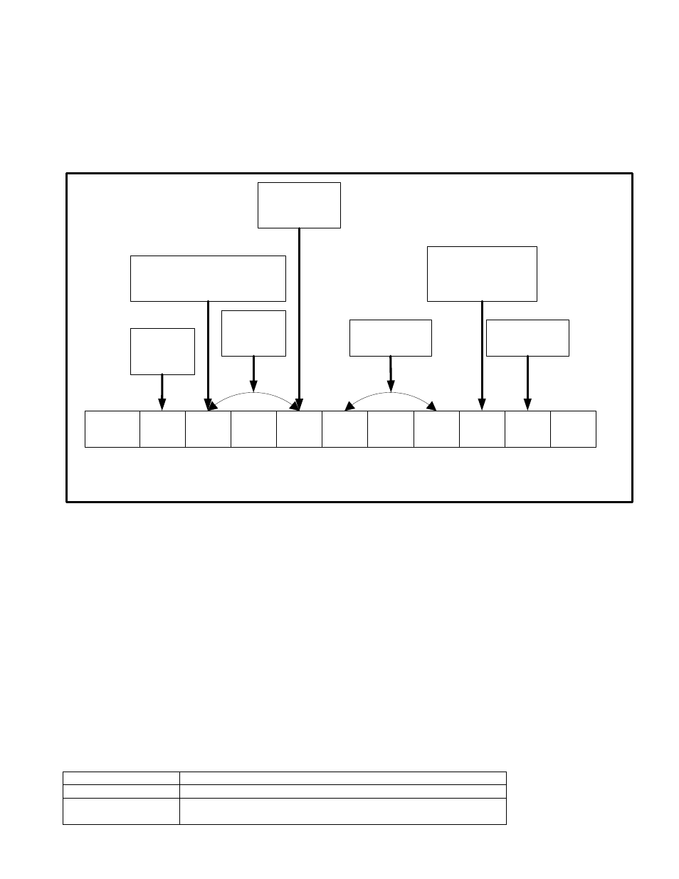
Figure 7-5 shows the ADC frame sequence for the following programmed sequence of ADC channels.
1. CH0: Average of 4 Samples
2. CH4: Average of 8 Samples
3. CH5: Average of 16 Samples
4. CH6: Average of 1 Sample
5. S/H0: Average of 2 Samples
6. S/H1: Average of 4 Samples
7. Internal Temperaute: Average of 16 Samples
CH0
(4)
CH4
(8)
S/H1
(4)
CH5
(16)
S/H0
(2)
CH6
(1)
Int
Temp
(1)
CH0
(4)
……..
……..
Every alternate
channel is
primary channel
Both S/H0 & S/H1 are ready. S/
H0 samples will get converted
by ADC and average value is
reported.
S/H1 samples
will get
converted by
ADC.
Sequence
keeps repeating
SH0 or 1 if
triggered by
internal or
SHEN0/1l
S/H0
(2)
End of Sequence.
One Sample of
Internal Temperature
gets chance here.
CH0
samples get
converted
by ADC
t = 0
t = 144µs
t = 216µs
t = 504µs
t = 648µs
t = 1224µs
t = 1338µs
t = 1296µs
t = 1332µs
t = 1512µs
Note: Conversion time is using the default clock.
Figure 7-5: ADC Frame Sequence with Averaging
7.1.10 – ADC Data Reading
The ADC has a circular data buffer that can hold the results from 25 conversions. When the location override
(LOC_OVR = 0) is disabled, the ADC controller writes the ADC conversion result at the data buffer location
corresponding to ADC channel number, see Table 7-1. When location override is enabled, the ADC controller writes
the result to the data buffer location configured in the ALT_LOC[4:0] bits in the ADDATA during ADC configuration
(ADST.ADCFG = 1). Using the location override feature, multiple conversions for a single channel can be stored to
data buffers as explained in example code 7.3.2. This buffer is accessed by reading the ADDATA register when
ADCFG is set to 0. The data buffer pointed to by ADST.ADIDX [4:0] is the buffer returned when ADDATA is read.
The ADIDX is automatically incremented following a read of ADDATA. This allows repeated reads of ADDATA to
return the results from multiple conversions. The ADC continues writing to the data buffer until the end of the buffer.
Once the end of the data buffer is reached, the ADC index rolls over and reading continues from data buffer 0.
7.1.11 – ADC Interrupts
The ADC Data Available Ready ADDAI bit in the ADST1 register is set when conversions are complete. This flag
generates an interrupt if enabled by setting the ADCN.ADDAIE interrupt enable bit. The condition that causes the
ADDAI flag to be set can be selected using the ADCN.ADDAINV bit.
Table 7-3: ADC Interrupt Intervals
ADDAINV
SET ADDAI AFTER
0
End of Every Sequence (ADSTART to ADEND)
1
After End of Every Sequence (ADSTART to ADEND) and After
(NUM_SMP + 1) ADC Conversions