Flash memory control register – Samsung S3F401F User Manual
Page 76
INTERNAL FLASH ROM
S3F401F_UM_REV1.00
5-16
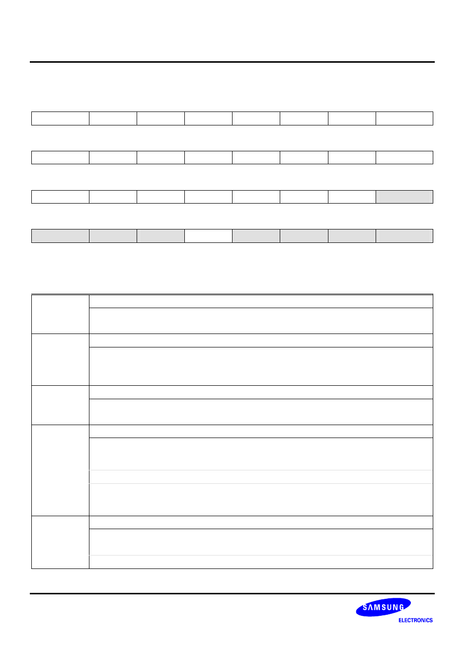
Flash Memory Control Register
FMUCON (0x00C)
Access: Read/Write
31 30 29 28 27 26 25 24
−
−
−
−
−
−
−
−
R/W-0 R/W-0 R/W-0 R/W-0 R/W-0 R/W-0 R/W-0 R/W-0
23 22 21 20 19 18 17 16
−
−
−
−
−
−
−
−
R/W-0 R/W-0 R/W-0 R/W-0 R/W-0 R/W-0 R/W-0 R/W-0
15 14 13 12 11 10 9
8
−
−
−
−
−
−
−
INTERLEAVE
R/W-0 R/W-0 R/W-0 R/W-0 R/W-0 R/W-0 R/W-0 R/W-0
7 6 5 4 3 2 1 0
UOSCEN
USTRSTPT
UOPGMR
−
UCPUH
UPGMR
USERSR
UCERSR
R/W-0 R/W-0 R/W-0 R/W-0 R/W-0 R/W-0 R/W-0 R/W-0
W: Write
R: Read
-0: 0 After reset
-1: 1 After reset
-U: Undefined after reset
UCERSR
Chip Erase Enable Bit
0 = Disable
1 = Enable
USERSR
Sector Erase Enable Bit
0 = Disable
1 = Enable
Note: This bit can be used in only user program mode.
UPGMR
Normal Program Enable Bit
0 = Disable
1 = Enable
UCPUH
CPU Hold Control Bit
0 = CPU work during Flash programming/erasing.
In this case, the flash programming/erasing code should not be on the internal flash ROM. The
advantage is that CPU can perform other tasks until the completion of an operation.
1 = CPU hold during Flash programming / erasing
Note: This bit can be used user and tool program mode. This bit can be read written data in specific
sequence. That mean’s although you write the ‘1’, when you read the register, the data will be ‘0’.
The
written data is affected at the time flash on-going, operation start bit is ‘1’.
UOPGMR
Option Program Enable Bit (For protection option setting)
0 = Disable
1 = Enable
Note: This bit can be used user and tool program mode.