4 read protection bit 27 – Samsung S3F401F User Manual
Page 71
S3F401F_UM_REV1.00
INTERNAL FLASH ROM
5-11
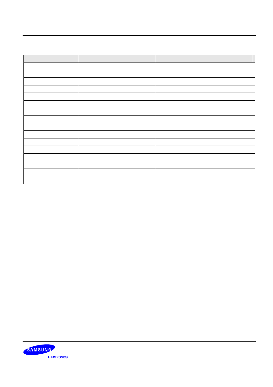
Table 5-4. Hardware Protection Area
FMDATA[15:0]
Hardware Protection Area Sector
Protected Area Address
0xFFFE
Sector 000 ~ Sector 015
0x0000_0000 ~ 0x0000_3FFF
0xFFFD
Sector 016~ Sector 031
0x0000_4000 ~ 0x0000_7FFF
0xFFFB
Sector 032~ Sector 047
0x0000_8000 ~ 0x0000_BFFF
0xFFF7
Sector 048~ Sector 063
0x0000_C000 ~ 0x0000_FFFF
0xFFEF
Sector 064~ Sector 079
0x0001_0000 ~ 0x0001_3FFF
0xFFDF
Sector 080~ Sector 095
0x0001_4000 ~ 0x0001_7FFF
0xFFBF
Sector 096~ Sector 111
0x0001_8000 ~ 0x0001_BFFF
0xFF7F
Sector 112~ Sector 127
0x0001_C000 ~ 0x0001_FFFF
0xFEFF
Sector 128~ Sector 143
0x0002_0000 ~ 0x0002_3FFF
0xFDFF
Sector 144~ Sector 159
0x0002_4000 ~ 0x0002_7FFF
0xFBFF
Sector 160~ Sector 175
0x0002_8000 ~ 0x0002_BFFF
0xF7FF
Sector 176~ Sector 191
0x0002_C000 ~ 0x0002_FFFF
0xEFFF
Sector 192~ Sector 207
0x0003_0000 ~ 0x0003_3FFF
0xDFFF
Sector 208~ Sector 223
0x0003_4000 ~ 0x0003_7FFF
0xBFFF
Sector 224~ Sector 239
0x0003_8000 ~ 0x0003_BFFF
0x7FFF
Sector 240~ Sector 255
0x0003_C000 ~ 0x0003_FFFF
5.4 READ PROTECTION BIT 27
Most users want that their data and code in memory would not be read by others. Read Protection can give the
solution for it by preventing the flash data from being read serially in the tool program mode.
When this function is enabled, reading the flash data in the tool program mode will result in all zero read-out. You
should write the proper data (refer to the above Protection Bit table) into the address 0x00000E3C. The address
0x00000E3C should be written the register FMADDR. The data consisting of protection bit should be written the
register FMDATA. As a next step, you should write the values (0x5A5A5A5A) into key register (FMKEY). Finally, set
FMUCON. Please refer to figure3. (Option Sector Program Flowchart)