Flash memory address register – Samsung S3F401F User Manual
Page 74
INTERNAL FLASH ROM
S3F401F_UM_REV1.00
5-14
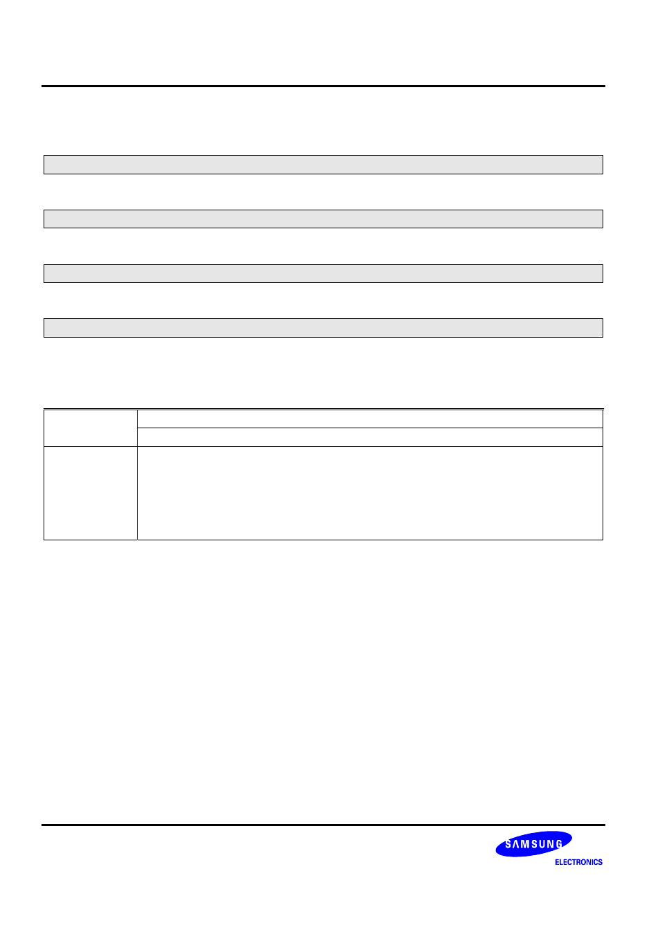
Flash Memory Address Register
FMADDR (0x004)
Access: Read/Write
31
30 29 28 27 26 25 24
FMADDRDAT [31:24]
R/W-0
R/W-0 R/W-0 R/W-0 R/W-0 R/W-0 R/W-0 R/W-0
23
22 21 20 19 18 17 16
FMADDRDAT [23:16]
R/W-0
R/W-0 R/W-0 R/W-0 R/W-0 R/W-0 R/W-0 R/W-0
15
14 13 12 11 10 9 8
FMADDRDAT [15:8]
R/W-0
R/W-0 R/W-0 R/W-0 R/W-0 R/W-0 R/W-0 R/W-0
7
6 5 4 3 2 1 0
FMADDRDAT [7:0]
R/W-0
R/W-0 R/W-0 R/W-0 R/W-0 R/W-0 R/W-0 R/W-0
W: Write
R: Read
-0: 0 After reset
-1: 1 After reset
-U: Undefined after reset
Flash Memory Address
FMADDRDAT
Flash program / sector erase address register data
NOTE
In option programming, set FMADDR to 0x0E38 (Smart Option = Real Address “E”) or 0xE3C
(Protection Option = Real Address “F”) and FMDATA by the appropriate value and start the write
operation.
FMADDR [31:0]
Å Address to be selected by user in flash memory range
FMADDR [31:0]
Å 0x00000E38 on programming smart option for hardware protection
FMADDR [31:0]
Å 0x00000E3C on programming protection option