Control register 0 – Samsung S3F401F User Manual
Page 216
S3F401F_UM_REV1.00
SSP
10-15
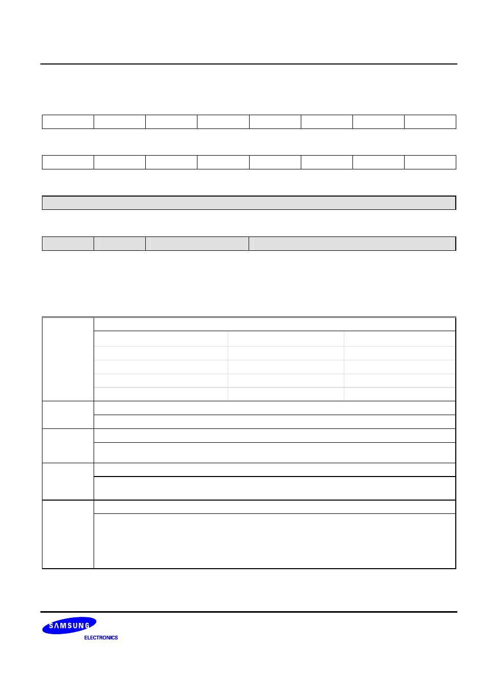
Control Register 0
SSPCR0 (0x000)
Access: Read/Write
31 30 29 28 27 26 25 24
−
−
−
−
−
−
−
−
R/W-0 R/W-0 R/W-0 R/W-0 R/W-0 R/W-0 R/W-0 R/W-0
23 22 21 20 19 18 17 16
−
−
−
−
−
−
−
−
R/W-0 R/W-0 R/W-0 R/W-0 R/W-0 R/W-0 R/W-0 R/W-0
15 14 13 12 11 10 9 8
SCR[15:8]
R/W-0 R/W-0 R/W-0 R/W-0 R/W-0 R/W-0 R/W-0 R/W-0
7 6 5 4 3 2 1 0
SPH
SPO
FRF[5:4]
DSS[3:0]
R/W-0 R/W-0 R/W-0 R/W-0 R/W-0 R/W-0 R/W-0 R/W-0
W: Write
R: Read
-0: 0 After reset
-1: 1 After reset
-U: Undefined after reset
DSS
Data Size Selection Field
0000~ 0010 = Reserved
0111 = 8-bit data
1100 = 13-bit data
0011 = 4-bit data
1000 = 9-bit data
1101 = 14-bit data
0100 = 5-bit data
1001 = 10-bit data
1110 = 15-bit data
0101 = 6-bit data
1010 = 11-bit data
1111 = 16-bit data
0110 = 7-bit data
1011 = 12-bit data
FRF
Frame Format Selection Field
Must be set to 00 for Motorola SPI frame format
SPO
SSPCLK Polarity Bit
0 = Data is captured on the first clock edge transition.
1 = Data is captured on the second clock edge transition.
SPH
SSPCLK Phase Selection Bit
0 = Data is captured on the first clock edge transition.
1 = Data is captured on the second clock edge transition
SCR
Serial Clock Rate Field
The value SCR is used to generate the transmit and receive bit rate.
The Bit Rate = F
PCLK
/ (CPSDVR x (1 + SCR))
Where CPSDVSR is an even value from 2 to 254, programmed through the SSPCPSR register
and SCR is a value from 0 to 255.