Pin descriptions – Samsung S3F401F User Manual
Page 23
S3F401F_UM_REV1.00
PRODUCT
OVERVIEW
1-9
5. PIN DESCRIPTIONS
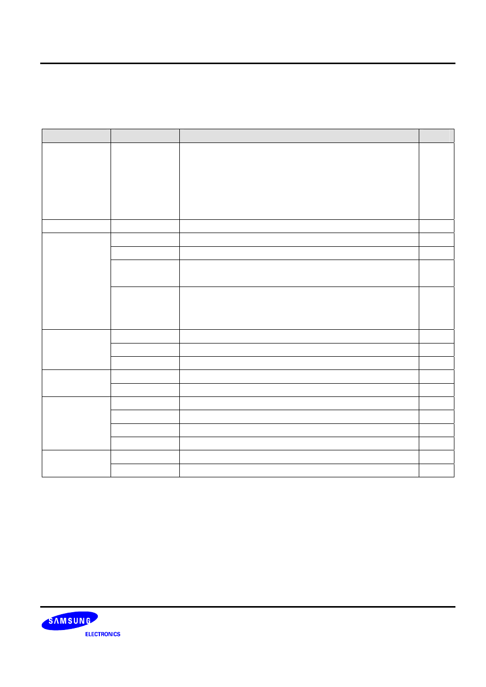
Table 1-2. S3F401F Pin Descriptions
Module
Pin Name
Description
I/O
The MD[2:0] can configure the operating mode of chip.
000 = Normal mode
001 = SPGM mode (Flash programming mode with writing tool)
Others = Test mode
BUS
CONTROLLER
MD[2:0]
Connect to GND through a 100nF capacitor with each mode
pin.
I
INTERRUPT INT[30:0]
External
interrupt request 31 to 0.
I
CLOCK &
Xin
Crystal input of oscillator circuit for system clock.
I
RESET
Xout
Crystal output of oscillator circuit for system clock.
O
Capacitor for PLL loop filter.
PLLCAP
Connect to GND through a
1200pF
capacitor
I
nRESET
Reset input: The global system reset input for the S3F401F.
For a system initialization, nRESET must be held to LOW level
for at least 1uSec. Connect to GND through
100nF
and
10nF
capacitor.
I
T[5:0]CLK
External clock input for Timer
I
T[5:0]CAP
Capture input for Timer
I
16-BIT TIMER
T[5:0]PWM
PWM output for Timer
O
UARTRXD[1:0]
UART receive
I
UART
UARTTXD[1:0]
UART transmit
O
SSPRXD[1:0] SSP
receive
I
SSPTXD[1:0] SSP
transmit
O
SSPCLK[1:0] SSP
clock
I/O
SSP
SSPFSS[1:0]
SSP frame input (for slave) / slave select output (for master)
I/O
AIN[14:0] ADC
input
AI
ADC
ADTRG
ADC trigger input
I