Port0 data status register – Samsung S3F401F User Manual
Page 174
S3F401F_UM_REV1.00
I/O
PORTS
8-25
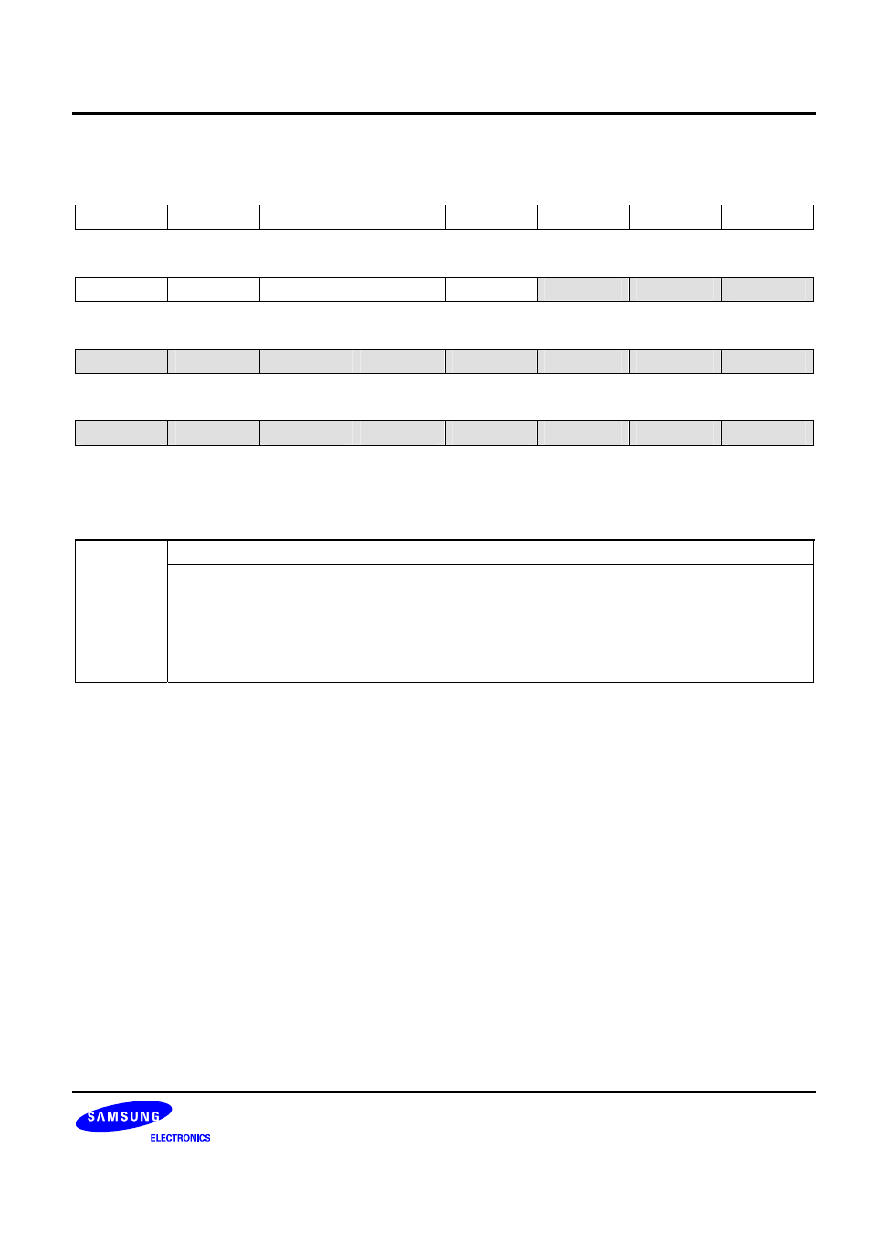
PORT0 Data Status Register
PDATSTAT0 (0x034) Access: Read Only
31 30 29 28 27 26 25 24
−
−
−
−
−
−
−
−
R-U R-U R-U R-U R-U R-U R-U R-U
23 22 21 20 19 18 17 16
−
−
−
−
−
P0.18
P0.17
P0.16
R-U R-U R-U R-U R-U R-U R-U R-U
15 14 13 12 11 10 9 8
P0.15
P0.14
P0.13
P0.12
P0.11
P0.10
P0.9
P0.8
R-U R-U R-U R-U R-U R-U R-U R-U
7 6 5 4 3 2 1 0
P0.7
P0.6
P0.5
P0.4
P0.3
P0.2
P0.1
P0.0
R-U R-U R-U R-U R-U R-U R-U R-U
W: Write
R: Read
-0: 0 After reset
-1: 1 After reset
: Undefined after reset
P0.[18:0]
Port 0 Output Data Status Bit
Port 0 output data status:
0: The real level of corresponding pin is at logic 0.
1: The real level of corresponding pin is at logic 1.
Values read from the address of this register reflect the external state of port 0 not the value
written to this register. Even though the port is configured as a functional pin except ADC, user
can know the external state of port 0 by reading this register.