Data register – Samsung S3F401F User Manual
Page 218
S3F401F_UM_REV1.00
SSP
10-17
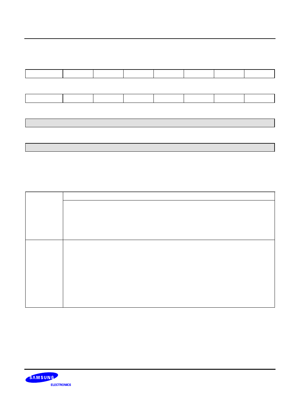
Data Register
SSPDR (0x008)
Access: Read/Write
31 30 29 28 27 26 25 24
−
−
−
−
−
−
−
−
R/W-0 R/W-0 R/W-0 R/W-0 R/W-0 R/W-0 R/W-0 R/W-0
23 22 21 20 19 18 17 16
−
−
−
−
−
−
−
−
R/W-0 R/W-0 R/W-0 R/W-0 R/W-0 R/W-0 R/W-0 R/W-0
15 14 13 12 11 10 9 8
DATA[15:8]
R/W-0 R/W-0 R/W-0 R/W-0 R/W-0 R/W-0 R/W-0 R/W-0
7 6 5 4 3 2 1 0
DATA[7:0]
R/W-0 R/W-0 R/W-0 R/W-0 R/W-0 R/W-0 R/W-0 R/W-0
W: Write
R: Read
-0: 0 After reset
-1: 1 After reset
-U: Undefined after reset
DATA Transmit/Receive
FIFO
Read = Receive FIFO
Write = Transmit FIFO
You must right-justify data when the PrimeCell SSP is programmed for a data size that is less
than 16 bits. Unused bits at the top are ignored by transmit logic. The receive logic automatically
right-justifies.
NOTE
When SSPDR is read, the entry in the receive FIFO (pointed to by the current FIFO read pointer) is
accessed. As data values are removed by the PrimeCell SSP receive logic from the incoming data frame,
they are placed into the entry in the receive FIFO (pointed to by the current FIFO write pointer).
When SSPDR is written to, the entry in the transmit FIFO (pointed to by the write pointer), is written to.
Data values are removed from the transmit FIFO one value at a time by the transmit logic. It is loaded into
the transmit serial shifter, then serially shifted out onto the SSPTXD pin at the programmed bit rate.
When a data size of less than 16 bits is selected, the user must right-justify data written to the transmit
FIFO. The transmit logic ignores the unused bits. Received data less than 16 bits is automatically
right-justified in their receive buffer.