2 transmit fifo, 3 transmit logic, 4 receive fifo – Samsung S3F401F User Manual
Page 245: 5 receive logic, 6 uart operation
S3F401F_UM_REV1.00
UART
12-7
3.2 TRANSMIT FIFO
The transmit FIFO is an 8-bit wide, 16 location deep, FIFO memory buffer. CPU data written across the APB
interface is stored in the FIFO until read out by the transmit logic. You can disable the transmit FIFO to act like a
one-byte holding register.
3.3 TRANSMIT LOGIC
The transmit logic performs parallel-to-serial conversion on the data read from the transmit FIFO. Control logic
outputs the serial bit stream beginning with a start bit, data bits with the Least Significant Bit (LSB) first, followed
by the parity bit, and then the stop bits according to the programmed configuration in control registers.
3.4 RECEIVE FIFO
The receive FIFO is a 12-bit wide, 16 location deep, FIFO memory buffer. Received data and corresponding error
bits, are stored in the receive FIFO by the receive logic until read out by the CPU across the APB interface. The
receive FIFO can be disabled to act like a one-byte holding register.
3.5 RECEIVE LOGIC
The receive logic performs serial-to-parallel conversion on the received bit stream after a valid start pulse has
been detected. Overrun, parity, frame error checking, and line break detection are also performed, and their
status accompanies the data that is written to the receive FIFO.
3.6 UART OPERATION
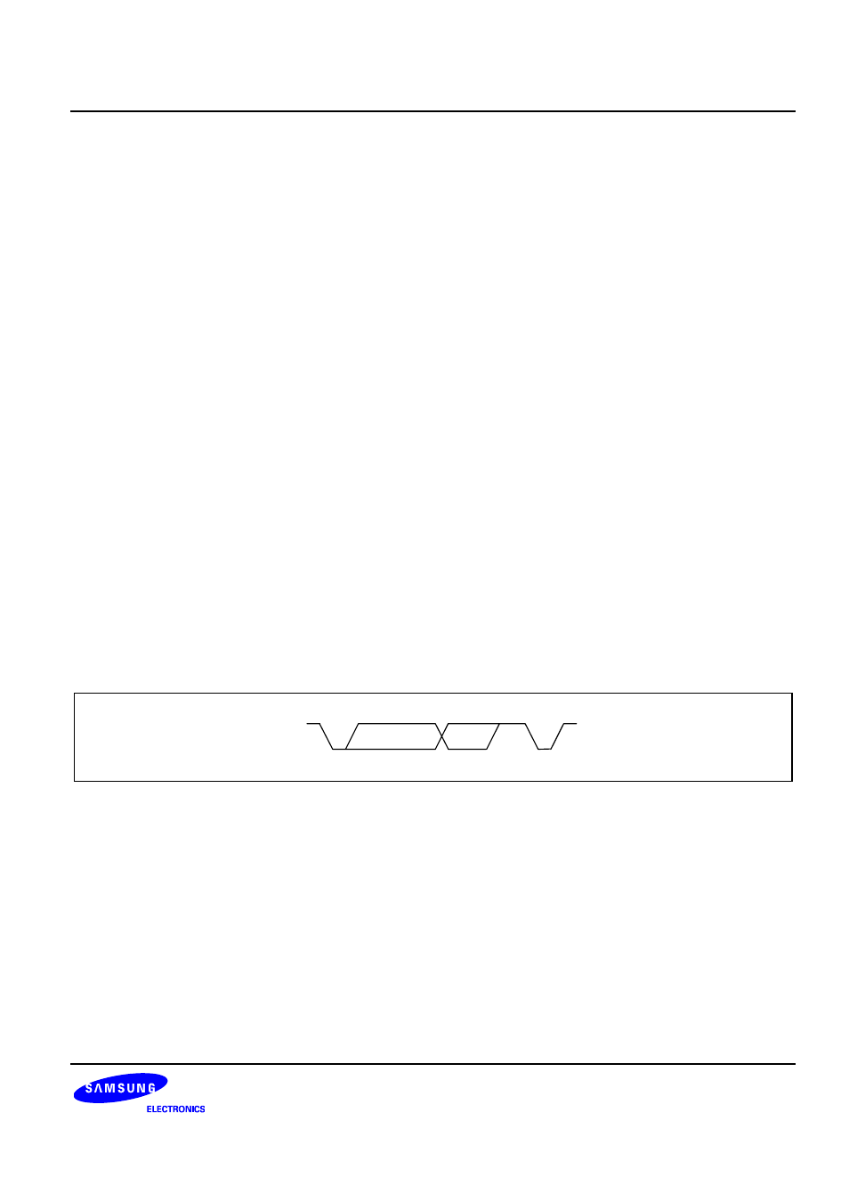
3.6.1 UART Character Frame
The UART character frame is shown next Figure.
5-8 data bits
Parity bit if
enabled
1-2
stop bits
n
Start
1
0
isb
msb
Figure 12-2. UART character frame