D figure 27, 78 sh – Echelon I/O Model Reference for Smart Transceivers and Neuron Chips User Manual
Page 88

78
Serial I/O Models
DATA OUT
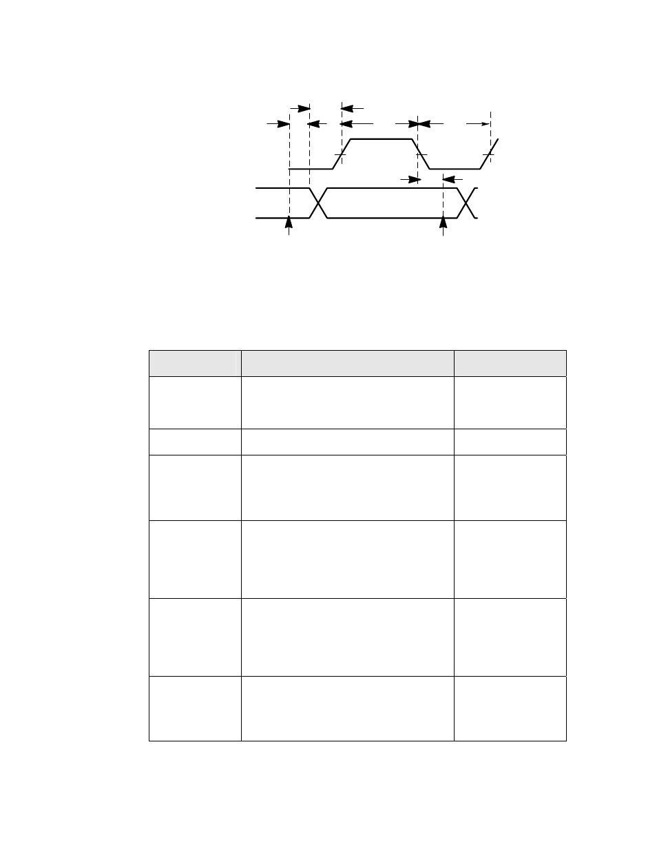
Active clock edge assumed to be positive in the above diagram.
OUTPUT
CLOCK
END OF
io_in()
START OF
io_in()
t
setup
t
fin
t
aet
t
tae
t
ret
Figure 27. Bitshift Output Timing
Table 31. Bitshift Output Latency Values for Series 3100 Devices
Symbol
Description
Typical at 10 MHz
t
fin
Function call to first data out stable
16-bit shift count
1-bit shift count
185.3 μs
337.6 μs
t
ret
Return from function
10.8 μs
t
setup
Data out stable to active clock edge
15 kbps bit rate
10 kbps bit rate
1 kbps bit rate
10.8 μs
10.8 μs
10.8 μs
t
aet
Active clock edge to next clock
transition
15 kbps bit rate
10 kbps bit rate
1 kbps bit rate
10.2 μs
42 μs
939.5 μs
t
tae
Clock transition to next active clock
edge
15 kbps bit rate
10 kbps bit rate
1 kbps bit rate
34.8 μs
34.8 μs
34.8 μs
f
Clock frequency = 1/(t
aet
+ t
tae
)
15 kbps bit rate
10 kbps bit rate
1 kbps bit rate
22 kHz
13 kHz
1.02 kHz
