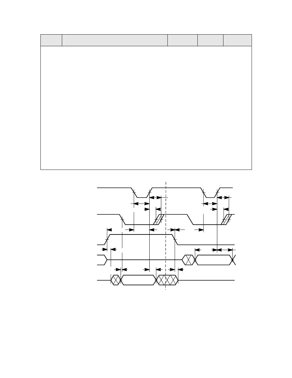
Figure 21 – Echelon I/O Model Reference for Smart Transceivers and Neuron Chips User Manual
Page 69

I/O Model Reference
59
Symbol Description
Minimum
Typical
Maximum
Notes:
1. XIN represents the period of the Smart Transceiver input clock (100 ns for a Series
3100 device at 10 MHz), or the period of the system clock for a Series 5000 device
(12.5 ns at 80 MHz).
2. Refer to the appropriate Neuron Chip or Smart Transceiver data sheet for detailed
measurement information.
3. For Smart Transceiver-to-Smart Transceiver operation, bus contention (t
mrdz
, t
sawdd
) is
eliminated by firmware, ensuring that a zero state is present when the token is
passed between the master and slave. See the
Parallel I/O Interface to the Neuron
Chip
engineering bulletin for additional information.
4. HS high is used as a slave busy flag. If HS is held low, the maximum data transfer
rate is 24 XIN per byte. If HS is not used for a flag, caution should be taken to
ensure that the master does not initiate a data transfer before the slave is ready.
5. Parameters were added to aid interface design with the Smart Transceiver.
6. Master holds output data valid during a write until the slave device pulls HS high.
7. In a master read, CS~ pulsing low acts like a handshake to flag the slave that data
has been latched in.
CS~
HS
R/W~
DATA OUT
DATA IN
READ CYCLE
(MASTER WRITE)
WRITE CYCLE
(MASTER READ)
t
sahsv
t
sacspw
t
sahsv
t
sacspw
t
sahsh
t
sarws
t
sarws
t
sahsh
t
sarwh
t
sards
t
sardh
t
sawd
t
sawds
t
sawdh
t
sardz
Figure 21. Slave A Mode Timing
