Echelon I/O Model Reference for Smart Transceivers and Neuron Chips User Manual
Page 46

36
Direct I/O Models
IO10
IO9
IO8
IO0
IO1
IO2
IO3
IO4
IO5
IO6
High Current Sink Drivers
Optional Pull-Up Resistors
IO10
IO9
IO8
IO0
IO1
IO2
IO3
IO4
IO5
IO6
IO7
IO7
IO11
IO11
Figure 10. Byte I/O for Series 3100 Devices
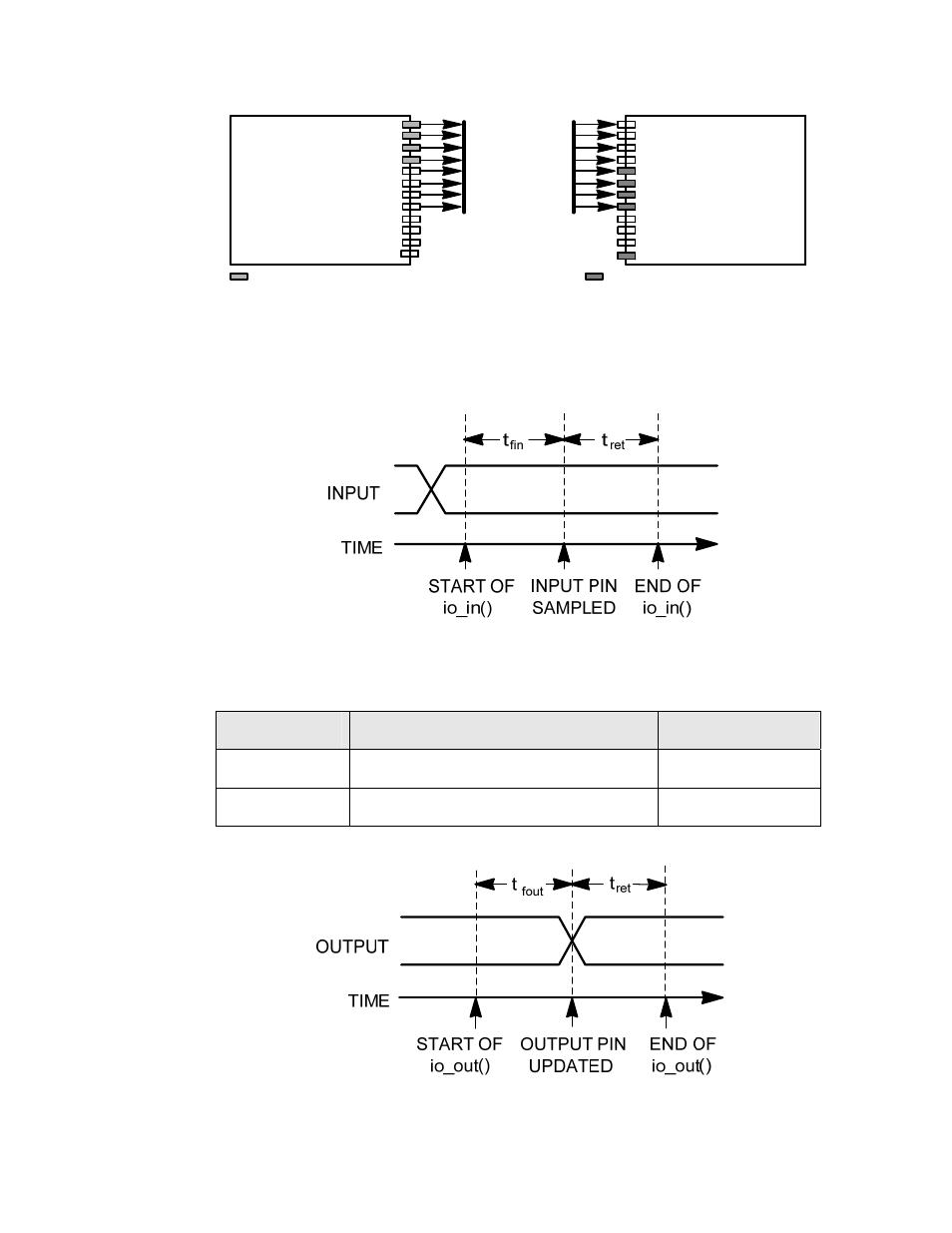
Figure 11 and Figure 12 show the byte input and byte output latency times,
respectively. These are the times from the call to the io_in() or io_out() function,
until a value is returned. The direction of bit ports can be changed between input
and output dynamically by using the io_set_direction() function.
Figure 11. Byte Input Timing
Table 13. Byte Input Latency Values for Series 3100 Devices
Symbol
Description
Typical at 10 MHz
t
fin
Function call to sample
24 μs
t
ret
Return from function
4 μs
Figure 12. Byte Output Timing
